 | –≠–ª–µ–∫—Ç—Ä–æ–Ω–Ω—ã–π –∫–æ–º–ø–æ–Ω–µ–Ω—Ç: LC72146M | –°–∫–∞—á–∞—Ç—å:  PDF PDF  ZIP ZIP |
CMOS LSI
Ordering number : EN4922C
73096HA (OT)/11095TH (OT) No. 4922-1/21
SANYO Electric Co.,Ltd. Semiconductor Bussiness Headquarters
TOKYO OFFICE Tokyo Bldg., 1-10, 1 Chome, Ueno, Taito-ku, TOKYO, 110 JAPAN
PLL Frequency Synthesizer
for Electronic Tuning
LC72146, 72146M
Overview
The LC72146 is a PLL frequency synthesizer LSI circuit
for electronic tuning in car stereo systems. The LC72146
supports the construction of high-performance, multi-
functional electronic tuning systems for the VHF MW,
and LW bands.
Features
∑ High-speed programmable dividers for
-- 10 to 160 MHz on FMIN using pulse swallower
-- 0.5 to 40.0 MHz on AMIN using pulse swallower
and direct division
∑ General-purpose counters
-- HCTR for 0.4 to 25.0 MHz frequency measurement
-- LCTR for 10 to 500 kHz frequency measurement
and 1.0 Hz to 20
◊
10
3
kHz period measurement
∑ Reference frequencies: Twelve selectable reference
frequencies (4.5 or 7.2 MHz crystal) 1, 3, 5, 9, 10,
3.125, 6.25, 12.5, 25, 30, 50 and 100 kHz
∑ Phase comparator
-- Insensitive band control
-- Unlock detection
-- Sub-charge pump for high-speed locking
-- Deadlock clear circuit
∑ CCB input/output data interface
∑ Power-on reset circuit
∑ Built-in MOS transistor for a low-pass filter
∑ Inputs/outputs (using five general-purpose input/output
ports)
-- Maximum of seven inputs (max)
-- Maximum of seven outputs (max/four n-channel
open-drain and three CMOS outputs)
-- Time-base output for clock (8 Hz)
∑ Operating ranges
-- Supply voltage ..................................4.5 to 5.5 V
-- Opetating temperature ......................≠40 to 85
∞
C
∑ Package
-- DIP24S, MFP24S
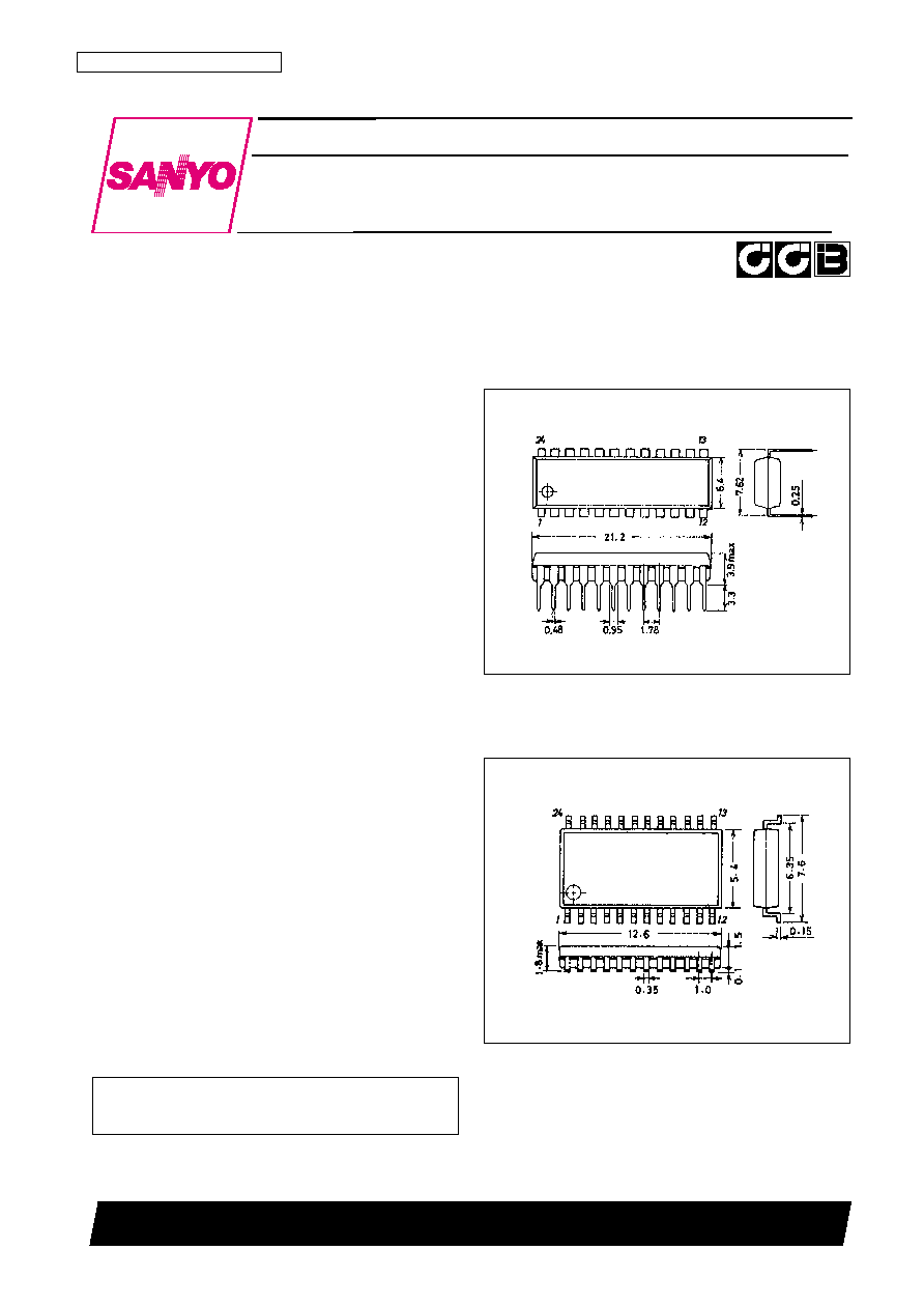
Package Dimensions
unit: mm
3067-DIP24S
unit: mm
3112-MFP24S
SANYO: DIP24S
[LC72146]
SANYO: MFP24S
[LC72146M]
∑ CCB is a trademark of SANYO ELECTRIC CO., LTD.
∑ CCB is SANYO's original bus format and all the bus
addresses are controlled by SANYO.
Specifications
Absolute Maximum Ratings
at Ta = 25
∞
C, V
SS
= 0 V
Allowable Operating Ranges
at Ta = ≠40 to 85∞C, V
SS
= 0 V
No. 4922-2/21
LC72146, 72146M
Parameter
Symbol
Conditions
min
typ
max
Unit
Supply voltage
V
DD
1
V
DD
4.5
5.5
V
V
DD
2
V
DD
: Serial data retain voltage
2.0
V
Input high-level voltage
V
IH
1
CE, CL, DI, I/O-1 to I/O-3
2.2
6.5
V
V
IH
2
I/O-4, I/O-5, HCTR/I-6 and LCTR/I-7
2.2
V
DD
V
Input low-level voltage
V
IL
1
CE, CL, DI and I/O-1 to I/O-5, HCTR/I-6, LCTR/I-7
0
0.8
V
Input high-leve lvoltage
V
IH
3
LCTR/I-7, Pulse wave
*
1
2.2
V
DD
V
Input low-level voltage
V
IL
2
LCTR/I-7, Pulse wave
*
1
0
0.8
V
Output voltage
V
O
1
DO
0
6.5
V
V
O
2
I/O-1 to I/O-3, AOUT, O-7
0
13
V
f
IN
1
XIN; Sine wave, capacitive coupling
1.0
8.0
MHz
f
IN
2
FMIN; Sine wave, capacitive coupling
10
160
MHz
Input frequency
f
IN
3
AMIN; Sine wave, capacitive coupling
0.5
40
MHz
f
IN
4
HCTR/I-6; Sine wave, capacitive coupling
0.4
25
MHz
f
IN
5
LCTR/I-7; Sine wave, capacitive coupling
10
500
kHz
f
IN
6
LCTR/I-7; Pulse wave, DC coupling
*
1
1.0
20
◊
10
3
Hz
Guaranteed oscillator
Xtal
XIN, XOUT; CI
120
4.0
8.0
MHz
element frequencies
V
IN
1
XIN
200
1500
mVrms
V
IN
2-1
FMIN; 50
f < 130 MHz
*
2
40
1500
mVrms
V
IN
2-2
FMIN; 10
f < 50 MHz
*
2
, 130
f 160 MHz
70
1500
mVrms
V
IN
3-1
AMIN; 2
f < 25 MHz
*
2
40
1500
mVrms
V
IN
3-2
AMIN; 25
f < 40 MHz
*
2
70
1500
mVrms
V
IN
3-3
AMIN; 0.5
f < 2.5 MHz
*
2
40
1500
mVrms
Input amplitude
V
IN
3-4
AMIN; 2.5
f < 10 MHz
*
2
70
1500
mVrms
V
IN
4-1
HCTR/I-6; 0.4
f < 25 MHz
*
3
40
1500
mVrms
V
IN
4-2
HCTR/I-6; 8
f < 12 MHz
*
4
70
1500
mVrms
V
IN
5-1
LCTR/I-7; 10
f < 400 kHz
*
3
40
1500
mVrms
V
IN
5-2
LCTR/I-7; 400
f < 500 kHz
*
3
20
1500
mVrms
V
IN
5-3
LCTR/I-7; 400
f < 500 kHz
*
4
70
1500
mVrms
Data set up time
t
SU
DI, CL
*
5
0.45
µS
Data hold time
t
HD
DI, CL
*
5
0.45
µS
Parameter
Symbol
Conditions
Ratings
Unit
Maximum supply voltage
V
DD
max
V
DD
≠0.3 to +7.0
V
V
IN
1 max
CE, CL, DI
≠0.3 to +7.0
V
Maximum input voltage
V
IN
2 max
XIN, FMIN, AIN, AMIN, HCTR/I-6, LCTR/I-7, I/O-4, I/O-5
≠0.3 to V
DD
+ 0.3
V
V
IN
3 max
I/O-1 to I/O-3
≠0.3 to +15
V
V
O
1 max
DO
≠0.3 to +7.0
V
Maximum output voltage
V
O
2 max
XOUT, I/O-4, I/O-5, O-6, PD0, PF1, AIN
≠0.3 to V
DD
+ 0.3
V
V
O
3 max
I/O-1 to I/O-3, AOUT, O-7
≠0.3 to +15
V
I
O
1 max
I/O-4, I/O-5, O-6, O-7
0 to 3.0
mA
Maximum output current
I
O
2 max
DO, AOUT
0 to 6.0
mA
I
O
3 max
I/O-1 to I/O-3
0 to 10
mA
Allowable power dissipation
Pd max
DIP24S:Ta
85∞C
350
mW
MFP24S:Ta
85∞C
220
mW
Operating temperature
Topr
≠40 to +85
∞C
Storage temperature
Tstg
≠55 to +125
∞C
Continued on next page.
Continued from preceding page.
Note: 1. Period measurement
2. See the description of the structure of the programmable divider.
3. With the CTC bit in the serial data set to 0
4. With the CTC bit in the serial data set to 1
5. See the description of the serial data timing.
Electrical Characteristics
at Ta = ≠40 to +85∞C, V
SS
= 0 V
No. 4922-3/21
LC72146, 72146M
Parameter
Symbol
Conditions
min
typ
max
Unit
Clock low-level time
t
CL
CL
*
5
0.45
µs
Clock high-level time
t
CH
CL
*
5
0.45
µs
CE wait time
t
EL
CE, CL
*
5
0.45
µs
CE setup time
t
ES
CL, CE
*
5
0.45
µs
CE hold time
t
EH
CE, CL
*
5
0.45
µs
Chip enable to data latch time
t
LC
*
5
0.45
µs
Data output time
t
DC
DO, CL; Depends on pull-up resistor
0.2
µs
Parameter
Symbol
Conditions
min
typ
max
Unit
Rf1
XIN
1.0
m
Rf2
FMIN
500
k
Internal feedback resistance
Rf3
AMIN
500
k
Rf4
HCTR/I-6
250
k
Rf5
LCTR/I-7
250
k
Sub charge pump
R1S
AIN
100
internal resistance
Hysteresis
V
HIS
CE, CL, DI, LCTR/I-7
0.1 V
DD
V
I
O
= 0.5 mA
V
DD
≠ 0.5
V
Output high-level voltage
V
OH
1
PD0, PD1, I/O-4, I/O-5, O-6
I
O
= 1 mA
V
DD
≠ 1.0
V
I
O
= 2 mA
V
DD
≠ 2.0
V
V
OH
2
AIN: I
O
= 1 mA
V
DD
≠ 0.6
V
DD
≠ 0.3
V
I
O
= 0.5 mA
0.5
V
V
OL
1
PD0, PD1, I/O-4,
I
O
= 1 mA
1.0
V
I/O-5, O-6, O-7
I
O
= 2 mA
2.0
V
V
OL
2
AIN: I
O
= 1 mA
0.3
0.6
V
Output low-level voltage
I
O
= 1 mA
0.2
V
V
OL
3
I/O-1 to I/O-3
I
O
= 2.5 mA
0.5
V
I
O
= 5 mA
1.0
V
I
O
= 9 mA
1.8
V
V
OL
4
DO; I
O
= 5 mA
1.0
V
V
OL
5
AOUT; I
O
= 1 mA, AIN = 1.3 V
0.5
V
I
IH
1
CE, CL, DI; V
I
= 6.5 V
5.0
µA
I
IH
2
I/O-1 to I/O-3; V
I
= 13 V
5.0
µA
Input high-level current
I
IH
3
I/O-4, I/O-5, HCTR/I-6, LCTR/I-7; V
I
= V
DD
5.0
µA
I
IH
4
XIN; V
I
= V
DD
2.0
11
µA
I
IH
5
FMIN, AMIN; V
I
= V
DD
4.0
22
µA
I
IH
6
HCTR/I-6, LCTR/I-7; V
I
= V
DD
8.0
44
µA
I
IL
1
CE, CL, DI; V
I
= 0 V
5.0
µA
I
IL
2
I/O-1 to I/O5; V
I
= 0 V
5.0
µA
Input low-level current
I
IL
3
HCTR/I-6, LCTR/I-7; V
I
= 0 V
5.0
µA
I
IL
4
XIN; V
I
= 0 V
2.0
11
µA
I
IL
5
FMIN, AMIN; V
I
= 0 V
4.0
22
µA
I
IL
6
HCTR/I-6, LCTR/I-7; V
I
= 0 V
8.0
44
µA
Continued on next page.
Continued from preceding page.
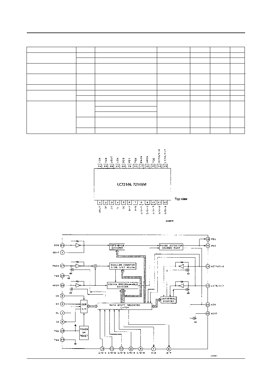
Pin Assignment
Block Diagram
No. 4922-4/21
LC72146, 72146M
Parameter
Symbol
Conditions
min
typ
max
Unit
Output off leakage current
I
OFF
1
I/O-1 to I/O3, AOUT, O-7; V
O
= 13 V
5.0
µA
I
OFF
2
DO; V
O
= 6.5 V
5.0
µA
High-level three state
I
OFFH
PD0, PD1, AIN; V
O
= V
DD
0.01
200
nA
off leakage current
Lowh-level three state
I
OFFL
PD0, PD1, AIN; V
O
= 0 V
0.01
200
nA
off leakage current
Input cacitance
C
IN
FMIN
6
pF
Pull-down transistor
R
pd
1
FMIN
80
200
600
k
on resistance
R
pd
2
AMIN
80
200
600
k
V
DD
; Xtal = 7.2 MHz, f
IN
2 = 160 MHz,
I
DD
1
V
IN
2 = 70 mVrms, f
IN
4 = 25 MHz
10
15
mA
Supply current
V
IN
4 = 40 mVrms
I
DD
2
V
DD
; PLL inhibited,
0.5
1.5
mA
crystal oscillator running (Xtal = 7.2 MHz)
I
DD
3
V
DD
; PLL inhibited, crystal oscillator stoped
10
µA
Pin Functions
No. 4922-5/21
LC72146, 72146M
Number
Symbol
Type
Function
Equivalent circuit
24
1
17
16
2
4
18
23
XIN
XOUT
Xtal OSC
FMIN
Local oscillator
signal input
AMIN
Local oscillator
signal input
CE
Chip enable
CL
Clock
DI
Input data
DO
Output data
V
DD
Power supply
V
DD
Ground
Connection for crystal oscillator element (7.2 or 4.5 MHz)
∑ Serial data input: FMIN is selected when DVS is set to 1.
Input frequency range: 10 to 160 MHz
∑ The signal is transmitted directly to the swallow counter
∑ Divisor value range: 272 to 65535
∑ Serial data input: AMIN is selected when DVS is set to 0.
∑ Serial data input: when SNS is set to 1.
∑ Input frequency range: 2 to 40 MHz
∑ The signal is transmitted directly to the swallow counter.
∑ Divisor value range: 272 to 65535
∑ Serial data input: when SNS is set to 0.
∑ Input frequency range: 0.5 to 10 MHz
∑ The signal is transmitted directly to the 12-bit
programmable divider.
∑ Divisor value range: 4 to 4095
12
11
10
I/O-1
I/O-2
I/O-3
General-purpose
I/O port
∑ General-purpose I/O ports
∑ Output mode circuit type: open drain
∑ Function after a power on reset: input port
∑ Can be set up to function as output ports by bits I/O-1 to
I/O-3 in the serial data sent from the controller.
∑ IThis pin must be set high to input serial data to the
LC72146 DI pin or to output serial data from the DO pin.
∑ Inputs the clock used for data synchronization when
inputting serial data to the LC72146 DI pin or outputting
serial data from the DO pin.
∑ Input pin for serial data transmitted to the LC72146 from
a controller.
∑ Output pin for serial data transmitted from the LC72146 to
a controller.
∑ The LC72146 power supply connection. A voltage
between 4.5 and 5.5 volts must be supplied when the
PLL circuit is used.
∑ The power on reset circuit operates when power is first
applied.
Continued on next page.
∑ The LC72146 ground connection.
3
15
5
Continued from preceding page.
Number
Symbol
Type
Function
Equivalent circuit
No. 4922-6/21
LC72146, 72146M
7
O-6
Output port
∑ The LC72146 latches the OUT6 bit in the serial data and
outputs it from pin O-6.
6
O-7
Output port
∑ The LC72146 latches the OUT7 bit in the serial data and
outputs it from pin O-7.
∑ Outputs a time base signal (8 Hz) when TBC is set to 1.
∑ Function after a power on reset: open circuit
9
8
I/O-4
I/O-5
General-purpose
I/O port
∑ General-purpose I/O ports
∑ Output mode circuit type: complementary
∑ Function after a power on reset: input port
∑ Can be set up to function as output ports by bits I/O-4
and I/O-5 in the serial data sent from the controller.
20
19
PD0
PD1
Charge pump
output
∑ PLL charge pump output pin
If the frequency generated by dividing the local oscillator
frequency by N is higher than the reference frequency, a
high level will be output from PD0, and if it is lower, a low
level will be output. PD0 goes to the high-impedance
state when the frequencies match.
∑ PD1 operates identically.
21
22
AIN
AOUT
Connections for the
low-pass filter
transistor
∑ Connections to the n-channel MOS transistor used for
the PLL active low-pass filter.
∑ A high-speed locking circuit can be formed by using
these pins with the built-in sub charge pump.
∑ See the item on the structure of the charge pump for
details.
Continued on next page.
14
HCTR/I-6
General-purpose
counter
∑ HCTR is selected when CTS1 is set to 1.
∑ Input frequency range: 0.4 to 25 MHz
∑ The signal is passed through a divide-by-two circuit and
then input to a general-purpose counter. This input also
supports an integrating count function.
∑ The result is output from the DO output pin starting with
the MSB of the general-purpose counter.
∑ See the item on the structure of the general-purpose
counter for details.
∑ When the H/I-6 bit in the serial data is set to 0:
∑ This pin functions as an input port, and the value input is
output from the DO pin.
No. 4922-7/21
LC72146, 72146M
Continued from preceding page.
Number
Symbol
Type
Function
Equivalent circuit
13
LCTR/I-7
General-purpose
counter
∑ LCTR is selected when CTS1 is set to 0.
∑ If the CTS0 bit in the serial data is set to 1:
∑ The circuit operates in frequency measurement mode.
∑ nput frequency range: 10 to 500 kHz
∑ The signal is directly transmitted to the general-purpose
counter without passing through the divide-by-two circuit.
∑ If the CTS0 bit in the serial data is set to 0:
∑ The circuit operates in period measurement mode.
∑
nput frequency range: 1 Hz to 20 kHz
∑ The measurement period can be set to be either one or
two periods of the input signal, and if two period
measurement is selected, the input frequency range
becomes 2 Hz to 40 kHz.
∑ The result is output from the DO output pin starting with
the MSB of the general-purpose counter.
∑ See the item on the structure of the general-purpose
counter for details.
∑ When the L/I-7 bit in the serial data is set to 0:
∑ This pin functions as an input port. The value input is
output from the DO pin.
Functional Description
Serial Data Input
The LC72146/72146M operating parameters are initialized by two 40-bit data words on the serial data input, DI, as
shown in Figure 1 and Figure 2 and Table 1.
Figure 1 Input Data Word IN1
Figure 2 Input Data Word IN2
No. 4922-8/21
LC72146, 72146M

Table 1 Input Data Functions
No. 4922-9/21
LC72146, 72146M
No.
Name
Function
Related bits
Programmable divider ratio
P15 is the MSB. The divider ratio, frequency range and lsb are determined by the setting of the DVS and
SNS flags as shown in Table 2 and Table 3. P0 to P3 are ignored if P4 is the LSB.
Table 2 Divider ratio settings
Note:
◊
= don't care
Table 3 Frequency range settings
Note:
◊
= don't care
Sub-charge pump control
Bits PDC0 and PDC1 control the charge pump state as shown in Table 4. The sub-charge pump is
connected to the gate of the low-pass filter transistor. This can be used in conjunction with PD0 and PD1
(main charge pump) to build a fast locking PLL.
Table 4 Charge pump state selection
Note:
◊
= don't care
*
See the "Charge Pump" on page 16 for details.
Reference frequency select
Bits R0 to R3 disable the PLL or select the reference frequency as shown in Table 5.
Table 5 Reference frequency selection
When the PLL is disabled, the programmable divider is stopped, AMIN and FMIN are pulled to ground,
and the charge-pump outputs become high impedance.
DVS
SNS
LSB
Divider ratio (N)
1
◊
P0
272 to 65535
0
1
P0
272 to 65535
0
0
P4
4 to 4095
DVS
SNS
Input port
Input frequency range (MHz)
1
◊
FMIN
10 to 160
0
1
AMIN
2 to 40
0
0
AMIN
0.5 to 10
PDC0
PDC1
Charge pump state
0
◊
High impedance
1
1
Operating (operates continuously)
1
0
Operating (when PLL is unlocked)
R
3
R
2
R
1
R
0
Reference frequency (kHz)
0
0
0
0
100
0
0
0
1
50
0
0
1
0
25
0
0
1
1
25
0
1
0
0
12.5
0
1
0
1
6.25
0
1
1
0
3.125
0
1
1
1
3.125
1
0
0
0
10
1
0
0
1
9
1
0
1
0
5
1
0
1
1
1
1
1
0
0
3
1
1
0
1
30
1
1
1
0
PLL inhibited and crystal oscillator stopped
1
1
1
1
PLL inhibited
P0 to P15,
DVS, SNS
(1)
PDC0,
PDC1
(2)
R0 to R3
(3)
UL0, UL1, DLC
Continued on next page.

Continued from preceding page.
No. 4922-10/21
LC72146, 72146M
No.
Name
Function
Related bits
DO and I/O5 output control data
Bits ULD, DT0, DT1, IL0 and IL1 control the mode of outputs DO and I/O5 as shown in Table 6 and Table 7.
Table 6 DO and I/O5 output flag selection
Note:
*
1. End-UC flags that general-purpose counter operation has finished.
*
2. Applicable only if I/O5 is set to be an output port.
Figure 3 DO output state
Table 7 IN state selection
Note: 1. If I/O1 or I/O2 is set to be an output port, IN becomes open.
2. DO does not go low when the crystal oscillator has stopped.
[When reference frequencies are as these: R3 = R2 = R1 = 1; R0 = 0]
Don't care.
Counter control
Bits CTS0 and CTS1 select the counter input as shown in Table 8.
Table 8 Counter input and measurement mode selection
Note:
◊
= don't care
Bit CTE starts the counter when 1, and resets the counter, when 0.
Bits GT0 and GT1 select the measurement time in frequency measurement mode or the number of
periods to count in period measurement mode as shown in Table 9.
Table 9 Measurement duration selection
When CTE is 0 the input is pulled down, and when CTP is 1 it is not. (Wait time: 1 to 2 ms.)
CTP must be set to 1 at least 4 ms before CTE is set to 1.
The input sensitivity can be reduced by setting CTC to 1. (Sensitivity: 10 to 30 mV rms)
(4)
ULD, DT0,
DT1, IL0, IL1
(6)
(5)
CTS0,
CTS1, CTE,
GT0, GT1
*
CTP, CTC
OUT5, I/O1, I/O2, I/O5
H/I6, L/I7
ULD
DT1
DT0
DO
I/O5
0
0
0
Unlock flag
0
0
1
Open
OUT5 flag
*
2
.
0
1
0
End-UC flag
*
1
.
0
1
1
IN. See table 7.
1
0
0
Open
1
0
1
Open
Unlock flag
*
2
.
1
1
0
End-UC flag
1
1
1
IN. See table 7.
IL1
IL0
IN state
0
0
Open
0
1
I1 input
1
0
I2 input
1
1
DO goes low when I1 changes.
CTS1
CTS0
Input
Measurement
mode
1
◊
HCTR
Frequency
0
1
LCTR
Frequency
0
0
LCTR
Period
Frequency measurement
Period measurement
GT1
GT0
Measurement
Wait time (ms)
Cycles
duration (ms)
0
0
4
3 to 4
1
0
1
8
1
0
32
7 to 8
2
1
1
64
Continued on next page.
Continued from preceding page.
No. 4922-11/21
LC72146, 72146M
No.
Name
Function
Related bits
Input/output port control
Bits I/O1 to I/O5 set the direction of the ports. Each pin is an input when the corresponding bit is 0,
and an output, when the bit is 1. All ports are set to be inputs after power-on reset.
Output port data
Bits OUT1 to OUT7 set the output values of the O-1 to O-7 output ports. Each output is open or high when
the corresponding bit is 1, and low, when the bit is 0. A bit is ignored if the corresponding port is an input
port or the unlock output.
Counter input control
Bits H/I-6 and L/I-7 select the operation of the HCTR/I-6 and LCTR/I-7 pins. When H/I-6 is 0, HCTR/I-6 is an
input port, and when H/I-6 is 1, HCTR/I-6 is the HCTR input. When L/I-7 is 0, LCTR/I-7 is an input port, and
when L/I-7 is 1, LCTR/I-7 is the LCTR input.
PLL unlock detect control
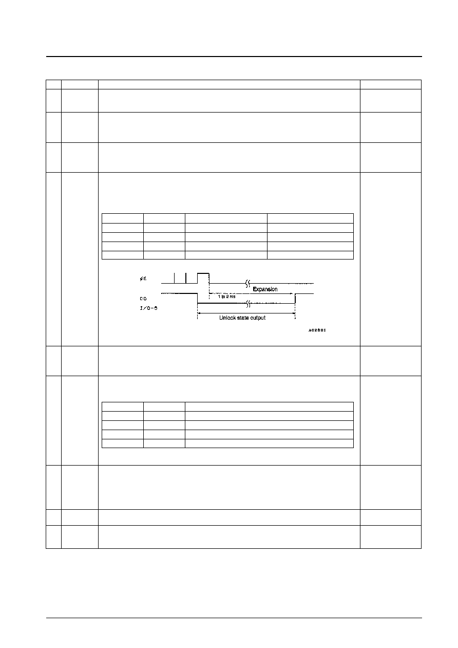
Bits UL0 and UL1 select the phase error threshold and extension (¯E) used to detect the PLL unlocked
state as shown in Table 10 and Figure 4. When the phase error is greater than the selected error, the PLL
unlock detector output goes low.
Table 10 Unlock detection and extension selection
Figure 4 Phase-error extension
Crystal oscillator control
Bit XS selects the oscillator frequency. When XS is 1, the frequency is 7.2 MHz, and when XS is 0,
4.5 MHz.
4.5 MHz is selected after power-on reset.
Phase comparator control
Bits DZ0 and DZ1 select the phase comparator insensitive band, or dead zone.
Table 11 Insensitive band mode selection
DZA is selected after power-on reset.
Charge pump control
Bit DLC controls the charge pump operation. When DLC is 1, the charge pump outputs are forced to low,
and when DLC is 0, the charge pump operates normally.
This feature can be useful to remove the PLL from a deadlock state. The PLL can deadlock if its VCO
control voltage V
tune
becomes 0 V, halting the VCO. Setting DLC to 1 sets V
tune
to V
CC
, restarting the VCO.
Normal operating mode is selected after power-on reset.
An 8 Hz 40% duty clock time base signal can be output from pins 0 to 7 by setting TBC to 1.
When TBC is 1 the OUT7 data will be invalid. TBC is set to 0 by the power-on reset.
Test data
Bits TEST0 to TEST2 are used for in-factory device testing. Set them all to 0. They are set to zero after a
power-on reset.
(7)
(8)
I/O1 to I/O5
OUT1 to
OUT7
(9)
H/I6, L/I7
(10)
UL0, UL1
(11)
XS
(12)
DZ0, DZ1
(15)
TEST0 to
TEST2
(14)
TBC
(13)
DLC
OUT1 to OUT5, ULD
I/O1 to I/O5, ULD
CTS0, CTS1
ULD, DT0, DT1
OUT7
UL1
UL0
Phase error
Detector output
0
0
Stopped
Open
0
1
0
¯E output
1
0
±0.56 µs
¯E with 1 to 2 ms extension
1
1
±1.11 µs
¯E with 1 to 2 ms extension
DZ1
DZ0
Insensitive band (dead zone) mode
0
0
DZA
0
1
DZB
1
0
DZC
1
1
DZD
Serial Data Output
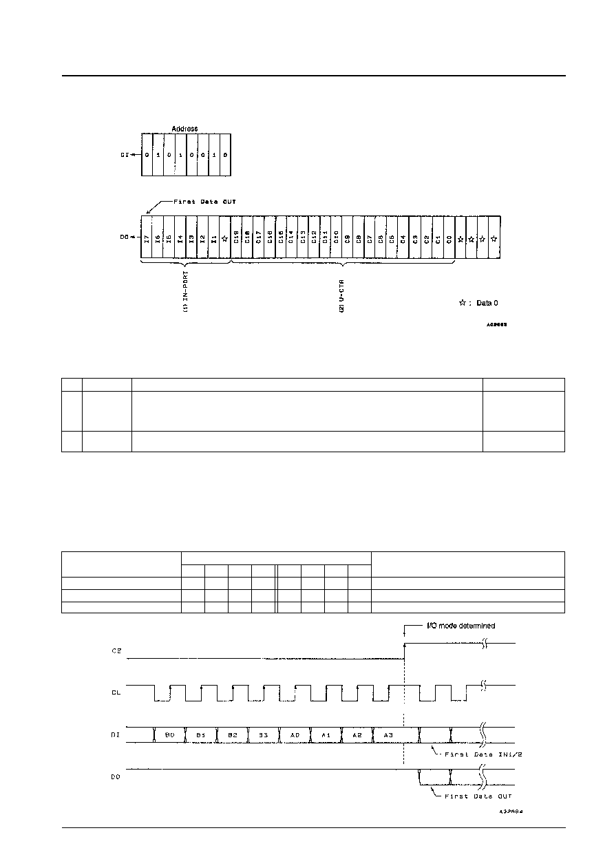
The 40-bit data word output on DO has the format and functions as shown in Figure 5 and Table 12, respectively.
Figure 5 Output Data Word Out
Table 12 Input Data Functions
Serial Data Input/Output Mode Selection
The LC72146/M use the CCB (computer control bus) serial data format. The first eight bits form the address, shown in
Figure 6, used to select the mode of operation as shown in Table 13.
Table 13 Serial Data Input/Output Mode Selection
No. 4922-12/21
LC72146, 72146M
No.
Name
Function
Related bits
Input port data
Bits I-1 to I-7 reflect the data latched into each input port when the device changes to data output mode.
I6 and I7 are zero when the corresponding port is a counter input. I1 to I5 correspond to the I/O1 to I/O5
ports, and I6 and I7, to the HCTR/I6 and LCTR/I7 inputs, respectively.
Counter contents
Bits C0 to C19 are the latched contents of the 20-bit binary counter. C19 is the msb. C0 is the lsb.
(1)
I1 to I7
(2)
C0 to C19
I/O-1 to I/O-5, H/I-6,
L/I-7
OUT1 to OUT5
CTS0, CTS1, CTE
Input/output mode
Address
Function
B0
B1
B2
B3
A0
A1
A2
A3
IN1
0
0
0
1
0
0
1
0
32-bit control data input
IN2
1
0
0
1
0
0
1
0
32-bit control data input
OUT
0
1
0
1
0
0
1
0
Output data. Data is output if the clock is active.

1. Serial data input (IN1/IN2)
2. Serial data output (OUT)
Note: 1. The data conversion time varies with the value of the pull-up resistor, since the DO pin is an n-channel open drain circuit.
2. The DO pin is normally open.
Programmable Divider
The configuration of the programmable divider is shown in Figure 7. The input mode selection is shown in Table 14, and
the input sensitivity, in Table 15.
Figure 7 Programmable Divider
Table 14 Programmable Divider Selection
Note:
◊
= don't care
No. 4922-13/21
LC72146, 72146M
DVS
SNS
Divisor setting (NO)
Input frequency range
Input port
1
◊
272 to 65535
10 to 160 MHz
FMIN
0
1
272 to 65535
2 to 40 MHz
AMIN
0
0
4 to 4095
0.5 to 10 MHz
AMIN
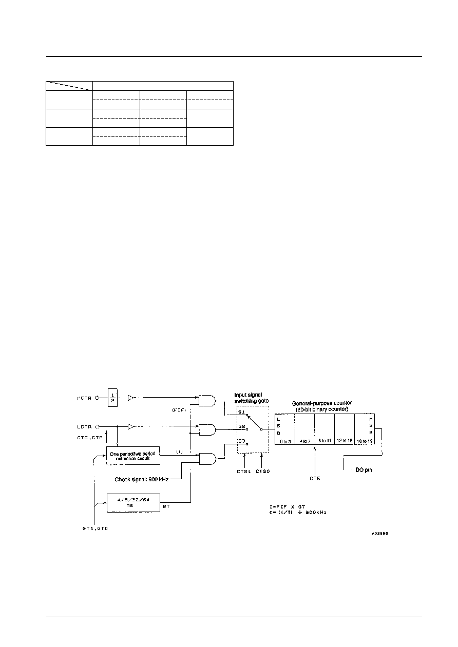
Table 15 Input Sensitivity (Target Sensitivity)
CTC: Input sensitivity switching data. When CTC is 1 the input sensitivity is degraded.However, the actual values will be:
HCTR
30 to 40 mVrms (frequency: 10.7 MHz)
LCTR
10 to 15 mVrms (frequency: 450 kHz)
CTP: The input pull-down resistor (when CTE is 0) can be disabled by setting CTP to 1.
CTP must be set to 1 at least 4 ms before CTE is set to 1. CTP should be set to 0 if the counter is not used.
When CTP is set to 1 wait time is reduced at 1 to 2 ms.
The LC72146 includes a general-purpose 20-bit binary counter whose value can be read out from the DO pin, msb first.
When using this counter for frequency measurement, one of four measurement times (4, 8, 32, or 64 ms) is selected by
GT0 and GT1. The frequency input to either the HCTR or the LCTR pin can be measured by determining the number of
pulses input to the counter during the measurement period.
This counter can be used to measure the period of the signal input to the LCTR pin by determining how many cycles of a
reference signal (900 kHz) are input to the counter during one or two periods of the LCTR pin signal.
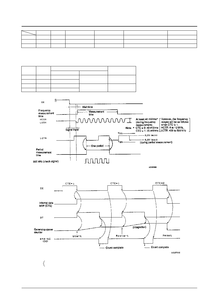
The counter is started by setting the serial data CTE bit to 1. While serial data is latched in the LC72146 when CE falls
from high to low, input to the HCTR or the LCTR pin must be provided within the waiting period that follows CE being
set low.
Next, after the measurement completes, the value of the counter must be read out during the period that CTE is 1. (The
general-purpose counter is reset when CTE is set to 0.)
It should be emphasized here that the counter should be reset before measurement by setting CTE to 0.
Also note that although the signal input to the LCTR pin is input to the counter directly, the signal input to the HCTR pin
is divided by two internally before being input to the counter. Accordingly, the value of the counter will be 1/2 the actual
frequency input to the HCTR pin.
Figure 8 General-Purpose Counter
No. 4922-14/21
LC72146, 72146M
Minimum input sensitivity (f [MHz])
(A) FMIN
10
f < 50
50
f < 130
130
f < 160
70 mVrms
40 mVrms
70 mVrms
(B) AMIN
2
f < 25
25
f < 40
--
40 mVrms
70 mVrms
(C) AMIN
0.5
f < 2.5
2.5
f < 10
--
40 mVrms
70 mVrms
Note:
*
CTC = 0: 40 mVrms
CTC = 1: 70 mVrms
However, the frequency ranges will be as follows when CTC is 1.
HCTR: 8 to 12 MHz, LCTR: 400 to 500 kHz
Integrating Count
Note: CTE: 0
∑ General-purpose counter reset
1
∑ General-purpose counter start
∑ Restarts on a new 1 setting
In integrated count mode, the count value is accumulated in the general-purpose counter.
Care is required to handle counter overflow.
Counter values: 0
H
to FFFFF
H
(1,048,575)
To implement the integrating count operation leave CTE set to 1. When the serial data (IN1) is transmitted again, the general-purpose counter will
start to measure the input again and the result will be added to the count.
No. 4922-15/21
LC72146, 72146M
CTS1
CTS0
Input pin
Measurement mode
Frequency range
Input sensitivity
S1
1
--
HCTR
Frequency
0.4 to 25.0 MHz
40 mVrms
*
S2
0
1
LCTR
Frequency
10 to 500 kHz
40 mVrms
*
S3
0
0
LCTR
Period
1.0 to 20
◊
10
3
Hz
(pulse)
GT1
GT0
Frequency measurement mode
Period measurement
Measurement time (ms)
Wait time (ms)
mode
0
0
4
3 to 4
One period
0
1
8
1
0
32
7 to 8
Two periods
1
1
64
Charge Pump
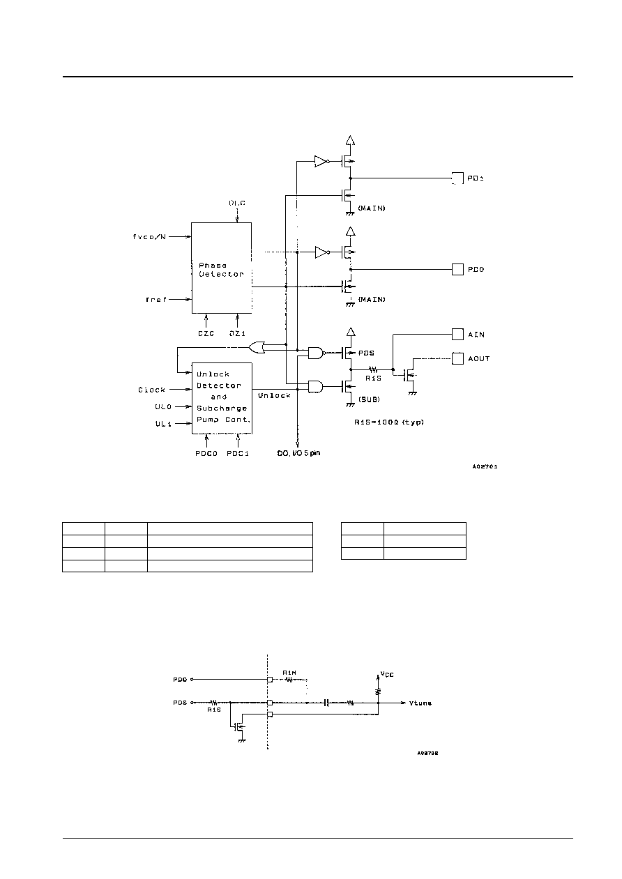
The charge pump configuration is shown in Figure 9.
Figure 9 Charge Pump
When unlock is detected following a channel change, PDS (the sub-charge pump) operates. The value of R1 changes to
R1M // R1S (R1S
100
), as shown in Figure 10, decreasing the low-pass filter time-constant and accelerating PLL
locking.
Figure 10 Charge Pump Connections
No. 4922-16/21
LC72146, 72146M
PDC1
PDC0
PDS (sub-charge pump state)
0
--
High impedance
1
1
Charge pump operates (normal operation)
1
0
Charge pump operates (when unlocked)
DLC
PD1, PD0, PDS
0
Normal operation
1
Forced to low
The unlock detection data UL1 must be set to 1. The unlock detection range will be set to ±0.56 µs or ±1.11 µs. If a
phase difference in excess of these values is detected the circuit will go to the unlock state and the sub-charge pump will
operate. When the circuit approaches the lock state and the phase difference falls under the unlock detection range, the
sub-charge pump operation will stop, i.e., the sub-charge pump will go to the high impedance state.
Note: 1. Notes on the phase comparator dead zone
Cases where the charge pump is in the ON/ON state require special care during system design since the charge
pump outputs correction pulses even when the PLL is locked and it is easy for the loop to become unstable.
The following problems may occur in the ON/ON state.
x Sidebands may be generated by reference frequency leakage.
y Sidebands may be generated by low frequency leakage due to the correction pulse envelope.
The settings that have a dead zone (the OFF/OFF settings) provide good loop stability, but it is hard to achieve
a good S/N ratio with these settings. Inversely, the settings with no dead zone (the ON/ON settings) allow a
high S/N ratio to be achieved but it is hard to achieve good loop stability with these settings.
Therefore, it can be effective to select either the DZA or DXB setting, i.e., a setting which has no dead zone,
when an S/N ratio of between 90 and 100 dB or higher is required in FM mode, or when the AM stereo pilot
margin needs to be increased. However, in cases where such a high FM S/N ratio is not required and where an
adequate AM stereo pilot margin can be achieved or AM stereo is not used, either the DZC or DZD setting,
i.e., a setting which has a dead zone, should be selected.
Dead Zone Definition
The phase comparator compares fp with a reference frequency (fr) as shown in Figure 11. Figure 12 shows the
characteristics of an ideal phase comparator, which outputs an output voltage (A) that is proportional to the
phase difference ¯. However, in an actual IC, a region (dead zone) in which minute phase differences cannot
be detected occurs due to internal circuit delays and other factors. To implement an end product with a high
S/N ration, the dead zone should be as small as possible.
However, there are cases where a larger dead zone can make a popularly-priced model easier to use. This is
because it is possible for RF leakage from the mixer to the VCO to modulate the VCO in popularly-priced
models when a strong RF input is applied. When the dead zone is small an output that compensates for this
problem is generated, and this output may itself modulate the VCO and generate beating with the RF
frequency.
No. 4922-17/21
LC72146, 72146M
DZ1
DZ0
Dead zone mode
Charge pump
Dead zone
0
0
DZA
ON/ON
≠ ≠0 s
0
1
DZB
ON/ON
≠0 s
1
0
DZC
OFF/OFF
+0 s
1
1
DZD
OFF/OFF
+ +0 s

Figure 11
Figure 12
2. FMIN, AMIN, HCTR and LCTR
These inputs should each be capacitively coupled using a 50 to 100 pF capacitor. Also, these capacitors should
be mounted as close as possible to their respective inputs.
3. IF counting using HCTR or LCTR
The LC72146 can perform IF count tuning when connected to an SD (station detector) signal from an IF IC.
IF counting should start when the SD signal becomes active.
Note on IF counting: The SD (station detect) signal must be used in conjunction with IF counting.
When using the general-purpose counter for IF counting, be sure to determine whether or not there is an SD
signal from the IF IC. The IF counter buffer should be turned on and IF counting performed only if there is an
SD signal. Autosearch techniques that use only the IF counter are not recommended, since it is possible for IF
buffer leakage output to cause incorrect stops at points where there is no station.
4. Using the DO pin
In modes other than data output mode, the DO pin is also used for counter completion, unlock detection, and for
checking for changes in the input pin. (In these cases the DO pin will change from the high to the low level.)
The state of the input pin can be input to the controller directly through the DO pin.
Pin States at Power On and Reset
No. 4922-18/21
LC72146, 72146M
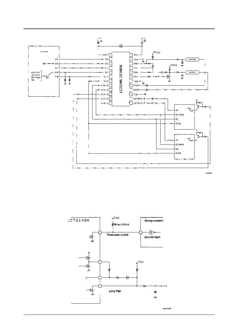
Application System Example
Note on Clock Time Base Usage
A resistor of at least 100 k
must be used as the clock time base output pin (O-7) pull-up resistor. Also, the use of a
Schmitt circuit is recommended in the controller (microprocessor) input circuit to prevent chattering. Forming a loop
filter with the built-in low-pass filter transistor will also serve to prevent degradation of the VCO C/N characteristics.
Since the grounding points for the clock time base output pin and the low-pass filter transistor are a common point
within the IC, current fluctuations in the clock time base output pin must be kept to a minimum to limit influencing the
low-pass filter.
No. 4922-19/21
LC72146, 72146M
No. 4922-20/21
LC72146, 72146M
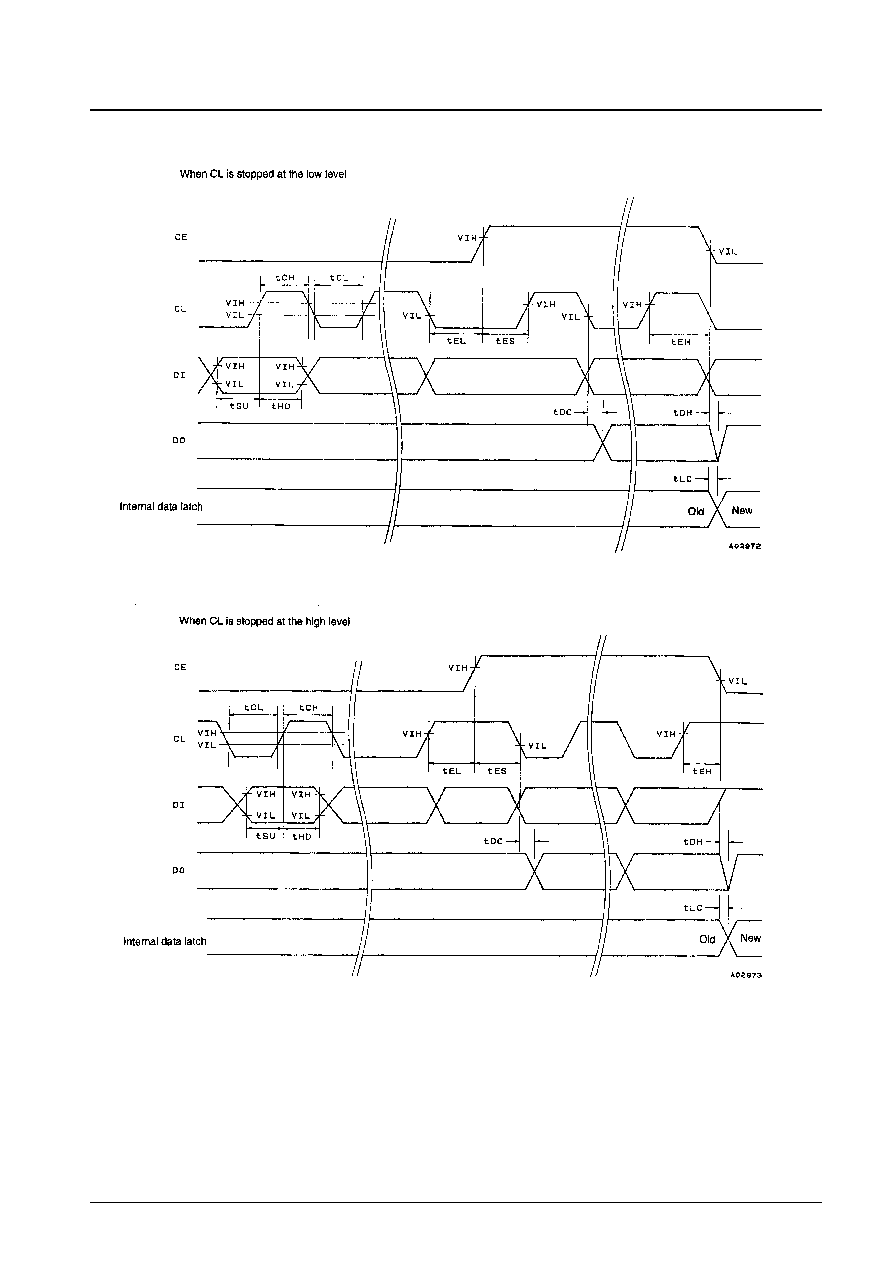
Serial Data Timing

No. 4925-21/21
LC72146, 72146M
This catalog provides information as of July, 1996. Specifications and information herein are subject to change
without notice.
s
No products described or contained herein are intended for use in surgical implants, life-support systems, aerospace
equipment, nuclear power control systems, vehicles, disaster/crime-prevention equipment and the like, the failure of
which may directly or indirectly cause injury, death or property loss.
s
Anyone purchasing any products described or contained herein for an above-mentioned use shall:
Accept full responsibility and indemnify and defend SANYO ELECTRIC CO., LTD., its affiliates, subsidiaries and
distributors and all their officers and employees, jointly and severally, against any and all claims and litigation and all
damages, cost and expenses associated with such use:
Not impose any responsibility for any fault or negligence which may be cited in any such claim or litigation on
SANYO ELECTRIC CO., LTD., its affiliates, subsidiaries and distributors or any of their officers and employees
jointly or severally.
s
Information (including circuit diagrams and circuit parameters) herein is for example only; it is not guaranteed for
volume production. SANYO believes information herein is accurate and reliable, but no guarantees are made or implied
regarding its use or any infringements of intellectual property rights or other rights of third parties.