 | –≠–ª–µ–∫—Ç—Ä–æ–Ω–Ω—ã–π –∫–æ–º–ø–æ–Ω–µ–Ω—Ç: LC72147V | –°–∫–∞—á–∞—Ç—å:  PDF PDF  ZIP ZIP |

Ordering number : ENN6675
O1300RM (OT) No. 6675-1/22
Overview
The LC72147V is a PLL frequency synthesizer for car
audio systems. It can implement high-performance
multifunction tuners and features a crystal oscillator
circuit that supports AM up-conversion, a fast locking
circuit, an A/D converter, and an LA1783/1750 IF counter
buffer control pin.
Functions
∑ High-speed programmable divider
-- FMIN: 10 to 180 MHz: Pulse swallower type
∑ IF counter
-- HCTR: 0.4 to 25 MHz: Frequency measurement
∑ Crystal oscillator: One of the following 4 frequencies
may be selected: 10.35, 10.25, 7.2, and 4.5 MHz
Reference frequency
-- One of 12 frequencies may be selected (when a 7.2
or 4.5 MHz crystal is used)
100
*1
, 50, 30
*2
, 25, 12.5, 6.25, 3.125, 10, 9
*2
, 5, 3
*2
,
1 kHz
Notes: 1. Cannot be used when a 10.35 or 10.25 MHz
crystal is used
2. Cannot be used when a 10.25 MHz crystal
is used
∑ Phase comparator
-- Supports dead band control
-- Built-in unlock detection circuit
-- Sub-charge pump for fast locking
-- Built-in deadlock clearing circuit
∑ Built-in MOS transistor for forming an active low-pass
filter
∑ I/O ports -- General-purpose I/O: 5 pins
-- Output: n-channel: 3 pins, CMOS: 2 pins
-- IFBC pin (LA1783/1750 IF counter buffer control
pin)
∑ Serial data I/O
-- Supports communication with the controller in the
CCB format.
∑ Operating ranges
-- Supply voltage (V
DD
): 4.5 to 6.5 V
-- Built-in regulator voltage (Vreg): 3.0 V (±10%)
-- Operating temperature: ≠40 to +85∞C
∑ Package
-- SSOP-24
Package Dimensions
unit: mm
3175A-SSOP24
1
12
13
7.6
8.0
0.5
5.6
0.1
1.6max
1.0
24
0.65
0.22
0.43
0.15
SANYO: SSOP24
[LC72147V]
LC72147V
SANYO Electric Co.,Ltd. Semiconductor Company
TOKYO OFFICE Tokyo Bldg., 1-10, 1 Chome, Ueno, Taito-ku, TOKYO, 110-8534 JAPAN
PLL Frequency Synthesizer for Electronic Tuning
in Car Audio Systems
CMOS IC
Any and all SANYO products described or contained herein do not have specifications that can handle
applications that require extremely high levels of reliability, such as life-support systems, aircraft's
control systems, or other applications whose failure can be reasonably expected to result in serious
physical and/or material damage. Consult with your SANYO representative nearest you before using
any SANYO products described or contained herein in such applications.
SANYO assumes no responsibility for equipment failures that result from using products at values that
exceed, even momentarily, rated values (such as maximum ratings, operating condition ranges, or other
parameters) listed in products specifications of any and all SANYO products described or contained
herein.
∑ CCB is a trademark of SANYO ELECTRIC CO., LTD.
∑ CCB is SANYO's original bus format and all the bus
addresses are controlled by SANYO.

Pin Assignment
No. 6675-2/22
LC72147V
I/O-5
HCTR
14
13
12
15
16
17
18
19
20
21
22
23
24
1
2
3
4
5
6
7
8
9
10
11
XOUT
IFBC
I/O-1
I/O-2
ADC0
ADC1
DO
CL
DI
CE
I/O-3
I/O-4
FMIN
XIN
Vreg
XBUF
AIN
PD
V
SS
V
DD
AV
SS
AOUT
Block Diagram
XBUF
PD
ADC1
ADC0
HCTR
AOUT
AIN
AV
SS
CE
FMIN
XOUT
XIN
DI
CL
DO
V
SS
V
DD
14 bits PROGRAMMABLE
REFERENCE
12 bits PROGRAMMABLE
DIVIDER
UNIVERSAL
COUNTER
PHASE DETECTOR
CHARGE PUMP
A/D
CONVERTER
DATA SHIFT REGISTER
LATCH
VOLTAGE
REGULATOR
3 V
POWER ON
RESET
CCB
I/F
SWALLOW COUNTER
1/16, 1/17 4 bits
1
24
12
23
15
7
PDS
10
9
22
21
20
4
6
5
16
17
2
11
13
I/O-5
I/O-4
I/O-3
I/O-2
I/O-1
Vreg
3
8
18
19
14
IFBC
No. 6675-3/22
LC72147V
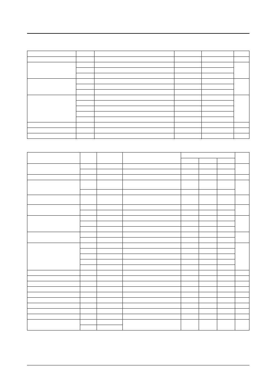
Parameter
Symbol
Pin
Conditions
Ratings
Unit
Supply voltage
V
DD
max
V
DD
≠0.3 to +7.0
V
V
IN
1 max
CE, CL, DI, AIN
≠0.3 to +7.0
Maximum input voltage
V
IN
2 max
XIN, FMIN, HCTR, I/O-4, I/O-5, ADC0, ADC1
≠0.3 to Vreg + 0.3
V
V
IN
3 max
I/O-1 to I/O-3
≠0.3 to +15
V
O
1 max
DO
≠0.3 to +7.0
Maximum output voltage
V
O
2 max
XOUT, IFBC, I/O-4, I/O-5, PD, XBUF
≠0.3 to Vreg + 0.3
V
V
O
3 max
I/O-1 to I/O-3, AOUT
≠0.3 to +15
I
O
1 max
IFBC
0 to 1.0
I
O
2 max
I/O-4, I/O-5, XBUF
0 to 3.0
Maximum output current
I
O
3 max
DO
0 to 6.0
mA
I
O
4 max
I/O-1 to I/O-3
0 to 10
I
O
5 max
AOUT
0 to 35
Allowable power dissipation
Pd max
Ta
85∞C
150
mW
Operating temperature
Topr
≠40 to +85
∞C
Storage temperature
Tstg
≠55 to +125
∞C
Specifications
Absolute Maximum Ratings
at Ta = 25∞C, V
SS
= 0 V
Note: Power supply V
DD
- V
SS
, Vreg - V
SS
: Capacitors of at least 2000 pF must be inserted between these pins when this device is used.
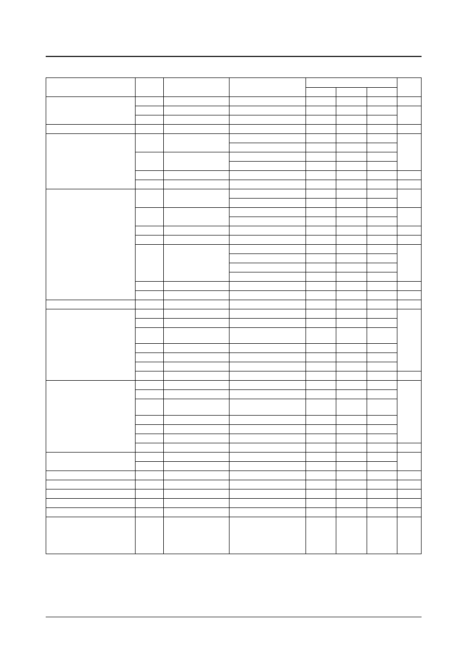
Parameter
Symbol
Pin
Conditions
Ratings
Unit
min
typ
max
Supply voltage
V
DD
1
V
DD
4.5
6.5
V
V
DD
2
V
DD
Serial data retention voltage
2.5
Regulator output voltage
Vreg
Vreg
4.5
V
DD
6.5 V
2.7
3.0
3.3
V
V
IH
1
CE, CL, DI,
2.2
6.5
V
High-level input voltage
I/O-1 to I/O-3
V
IH
2
I/O-4, I/O-5
2.2
Vreg
Low-level input voltage
V
IL
CE, CL, DI,
0
0.8
V
I/O-1 to I/O-5
Output voltage
V
O
1
DO
0
6.5
V
V
O
2
I/O-1 to I/O-3
0
13
f
IN
1
XIN
Sine wave, capacitance coupled
1.0
8.0
Input frequency
f
IN
2
FMIN
Sine wave, capacitance coupled
10
180
MHz
f
IN
3
HCTR
Sine wave, capacitance coupled
0.4
25
Guaranteed crystal oscillator
X'tal1
XIN, XOUT
*
1
4.0
7.0
MHz
frequency ranges
X'tal2
XIN, XOUT
*
1
7.1
10.5
V
IN
1
XIN
200
900
V
IN
2-1
FMIN
10
f < 130 MHz
*
2
40
900
Input amplitude
V
IN
2-2
FMIN
130
f
180 MHz
*
2
70
900
mVrms
V
IN
3-1
HCTR
0.4
f
25 MHz
*
3
70
900
V
IN
3-2
HCTR
8
f
12 MHz
*
4
100
900
Input voltage range
V
IN
4
ADC0, ADC1
0
Vreg
V
Data setup time
t
SU
DI, CL
*
5
0.45
µs
Data hold time
t
HD
DI, CL
*
5
0.45
µs
Clock low-level period
t
CL
CL
*
5
0.45
µs
Clock high-level period
t
CH
CL
*
5
0.45
µs
CE wait time
t
EL
CE, CL
*
5
0.45
µs
CE setup time
t
ES
CE, CL
*
5
0.45
µs
CE hold time
t
EH
CE, CL
*
5
0.45
µs
Data latch change time
t
LC
*
5
0.45
µs
Data output time
t
DC
DO, CL
Depends on the value of the pull-up
0.2
µs
t
DH
DO, CE
resistor used.
Allowable Operating Ranges
at Ta = ≠40 to 85∞C, V
SS
= 0 V
Notes:1. Recommended crystal oscillator CI values
CI
120
(Crystal: 4.5 MHz), CI
70
(Crystal: 7.2, 10.25, or 10.35 MHz)
Note that the crystal oscillator circuit characteristics depend on the printed circuit board and the particular components used. We recommend
consulting the manufacturer of the crystal when designing this circuit.
2. Refer to the description of the structure of the programmable divider.
3. Serial data: CTC = 0
4. Serial data: CTC = 1
5. See the timing chart for serial data transfers.
No. 6675-4/22
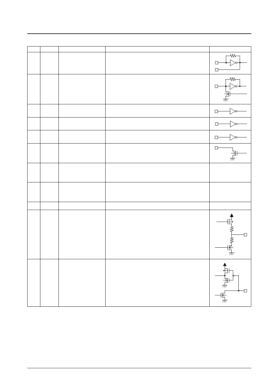
LC72147V
Parameter
Symbol
Pin
Conditions
Ratings
Unit
min
typ
max
Rf1
XIN
1.0
M
Internal feedback resistance
Rf2
FMIN
500
k
Rf3
HCTR
250
Hysteresis
V
HIS
CE, CL, DI
0.1 Vreg
V
V
OH
1
I/O-4, I/O-5
I
O
= ≠ 0.5 mA
Vreg ≠ 0.5
I
O
= ≠ 1 mA
Vreg ≠ 1.0
V
High-level output voltage
V
OH
2
PD, AIN
I
O
= ≠ 1 mA
Vreg ≠ 0.5
I
O
= ≠ 2 mA
Vreg ≠ 1.0
V
OH
3
XBUF
I
O
= ≠ 0.5 mA
Vreg ≠ 0.5
V
V
OH
4
IFBC
I
O
= ≠ 0.1 mA
Vreg ≠ 0.5
V
V
OL
1
I/O-4, I/O-5
I
O
= 0.5 mA
0.5
V
I
O
= 1 mA
1.0
V
OL
2
PD, AIN
I
O
= 1 mA
0.5
V
I
O
= 2 mA
1.0
V
OL
3
XBUF
I
O
= 0.5 mA
0.5
V
Low-level output voltage
V
OL
4
IFBC
I
O
= 0.1 mA
0.5
V
I
O
= 1 mA
0.2
V
OL
5
I/O-1 to I/O-3
I
O
= 2.5 mA
0.5
V
I
O
= 5 mA
1.0
I
O
= 9 mA
1.8
V
OL
6
DO
I
O
= 5 mA
1.0
V
V
OL
7
AOUT
I
O
= 30 mA, AIN = 2.0 V
1.5
V
Mid-level output voltage
V
OM
IFBC
I
O
= 20 µA
1.2
1.5
1.8
V
I
IH
1
CE, CL, DI
V
I
= 6.5 V
5.0
I
IH
2
I/O-1 to I/O-3
V
I
= 13 V
5.0
I
IH
3
I/O-4, I/O-5, ADC0,
V
I
= Vreg
5.0
µA
High-level input current
ADC1, HCTR
I
IH
4
XIN
V
I
= Vreg
1.3
7
I
IH
5
FMIN
V
I
= Vreg
2.5
14
I
IH
6
HCTR
V
I
= Vreg
5.0
28
I
IH
7
AIN
V
I
= Vreg
200
nA
I
IL
1
CE, CL, DI
V
I
= 0 V
5.0
I
IL
2
I/O-1 to I/O-3
V
I
= 0 V
5.0
I
IL
3
I/O-4, I/O-5,
V
I
= 0 V
5.0
µA
Low-level input current
ADC0, ADC1, HCTR
I
IL
4
XIN
V
I
= 0 V
1.3
7
I
IL
5
FMIN
V
I
= 0 V
2.5
14
I
IL
6
HCTR
V
I
= 0 V
5.0
28
I
IL
7
AIN
V
I
= 0 V
200
nA
Output off leakage current
I
OFF
1
I/O-1 to I/O-3
V
O
= 13 V
5.0
µA
I
OFF
2
DO
V
O
= 6.5 V
5.0
High-level 3-state off leakage current
I
OFFH
PD
V
O
= Vreg
0.01
200
nA
Low-level 3-state off leakage current
I
OFFL
PD
V
O
= 0 V
0.01
200
nA
Input capacitance
C
IN
FMIN
6
PF
A/D converter linearity error
Err
ADC0, ADC1
≠1/2
1/2
LSB
Pull-down transistor on resistance
Rpd
FMIN
80
200
600
k
X'tal = 10.35 MHz
f
IN
2 = 180 MHz
Supply current
I
DD
V
DD
V
IN
2 ≠ 2 = 70 mVrms
12
mA
f
IN
3 = 25 MHz
V
IN
3 ≠ 1 = 70 mVrms
Electrical Characteristics
in the Allowable Operating Ranges
No. 6675-5/22
LC72147V
Pin Functions
Pin No.
Symbol
Usage
Function
Pin circuit
∑ Crystal oscillator connection.
(4.5, 7.2, 10.25, or 10.35 MHz)
1
24
XIN
XOUT
X'tal OSC
∑ FMIN is selected by setting DVS in the control data to 1.
∑ Input frequency: 10 to 180 MHz
∑ The signal is transmitted to the swallow counter.
∑ The divisor can be set to a value in the range 272 to 65,535.
12
FMIN
Local oscillator signal input
∑ This pin must be set to the high level when inputting serial data to the
LC72147V DI pin and when outputting serial data from the DO pin.
23
CE
Chip enable
S
∑ Data synchronization clock signal used when inputting serial data to
the LC72147V DI pin and when outputting serial data from the DO pin.
21
CL
Clock
S
∑ Serial data input for transferring data from the controller to the
LC72147V.
22
DI
Input data
S
∑ Serial data output for transferring data from the LC72147V to the
controller.
20
DO
Output data
∑ LC72147V power supply. A voltage in the range 4.5 to 6.5 V must be
provided when the PLL circuit is operating.
∑ The power-on reset circuit operates when power is first applied.
------
------
------
4
V
DD
Power
∑ Regulator output. A capacitor must be inserted between Vreg and
V
SS
.
∑ The output voltage (3.0 V ±10%) is supplied to internal circuits.
5
Vreg
Regulator output
∑ LC72147V ground.
6
V
SS
Ground
∑ The LC72147V can control the LA1783/1750 IF buffer output.
∑ This is a 3-state output. (0 V, Vreg/2 = 1.5 V, and Vreg = 3 V)
14
IFBC
IF buffer control
∑ General-purpose I/O ports.
∑ The outputs are open-drain circuits.
∑ After the power-on reset, I/O-1 and I/O-2 function as input ports. I/O-
3 functions as an output port fixed at the low level.
∑ The input/output state of these ports can be set using the I/O-1 to
I/O-3 bits in the serial data sent from the controller.
16
17
2
I/O-1
I/O-2
I/O-3
General-purpose I/O ports
Continued on next page.