 | –≠–ª–µ–∫—Ç—Ä–æ–Ω–Ω—ã–π –∫–æ–º–ø–æ–Ω–µ–Ω—Ç: LC72148V | –°–∫–∞—á–∞—Ç—å:  PDF PDF  ZIP ZIP |
Ordering number : ENN6974A
41202RM (OT)/70601RM (OT) No. 6974-
Overview
The LC72148V is a 3 V version of the LC72146 PLL
frequency synthesizer that can easily implement a variety
of 3 V power supply tuners, including in-car navigation
system receivers based on the VICS FM multiplex system.
Functions
∑ High-speed programmable divider
-- FMIN: 10 to 180 MHz ... Pulse swallower technique
-- AMIN: 2 to 40 MHz ... Pulse swallower technique
0.5 to 10 MHz ... Direct division technique
∑ IF counters
-- HCTR: 0.4 to 25 MHz ... Frequency measurement
-- LCTR: 10 to 500 kHz ... Frequency measurement
1.0 to 20
◊
10
3
Hz ... Period measurement
∑ Reference frequency
-- One of 12 reference frequencies can be selected
(Crystal resonator: 7.2 or 4.5 MHz)
1, 3, 5, 9, 10, 3.125, 6.25, 12.5, 25, 30, 50, and
100 kHz
∑ Phase comparator
-- Provides dead zone control
-- Built-in unlock detection circuit
-- Built-in deadlock clear circuit
-- Sub-charge pump for high-speed locking
∑ Built-in MOS transistor for implementing an active low-
pass filter
∑ I/O ports: Five general-purpose I/O ports.
-- Input: 7 pins (maximum)
-- Output: 7 pins (maximum. N-channel: 4 pins,
CMOS: 3 pins)
-- A clock time base signal (8 Hz) can be output.
∑ Serial data I/O
-- Supports communication with a controller in the
CCB format.
-- Uses the same serial data as the LC72146.
∑ Operating ranges
-- Supply voltage: 2.7 to 3.6 V
-- Operating temperature: ≠40 to +85∞C
∑ Package
-- SSOP24
Package Dimensions
unit: mm
3175B-SSOP24
1
7.6
7.8
0.5
5.6
0.1
1.5max
24
0.65
0.22
(0.33)
0.15
(1.3)
SANYO: SSOP24
[LC72148V]
LC72148V
SANYO Electric Co.,Ltd. Semiconductor Company
TOKYO OFFICE Tokyo Bldg., 1-10, 1 Chome, Ueno, Taito-ku, TOKYO, 110-8534 JAPAN
Electronic Tuning PLL Frequency Synthesizer
for Car Stereo Systems
CMOS IC
Any and all SANYO products described or contained herein do not have specifications that can handle
applications that require extremely high levels of reliability, such as life-support systems, aircraft's
control systems, or other applications whose failure can be reasonably expected to result in serious
physical and/or material damage. Consult with your SANYO representative nearest you before using
any SANYO products described or contained herein in such applications.
SANYO assumes no responsibility for equipment failures that result from using products at values that
exceed, even momentarily, rated values (such as maximum ratings, operating condition ranges, or other
parameters) listed in products specifications of any and all SANYO products described or contained
herein.
∑ CCB is a trademark of SANYO ELECTRIC CO., LTD.
∑ CCB is SANYO's original bus format and all the bus
addresses are controlled by SANYO.
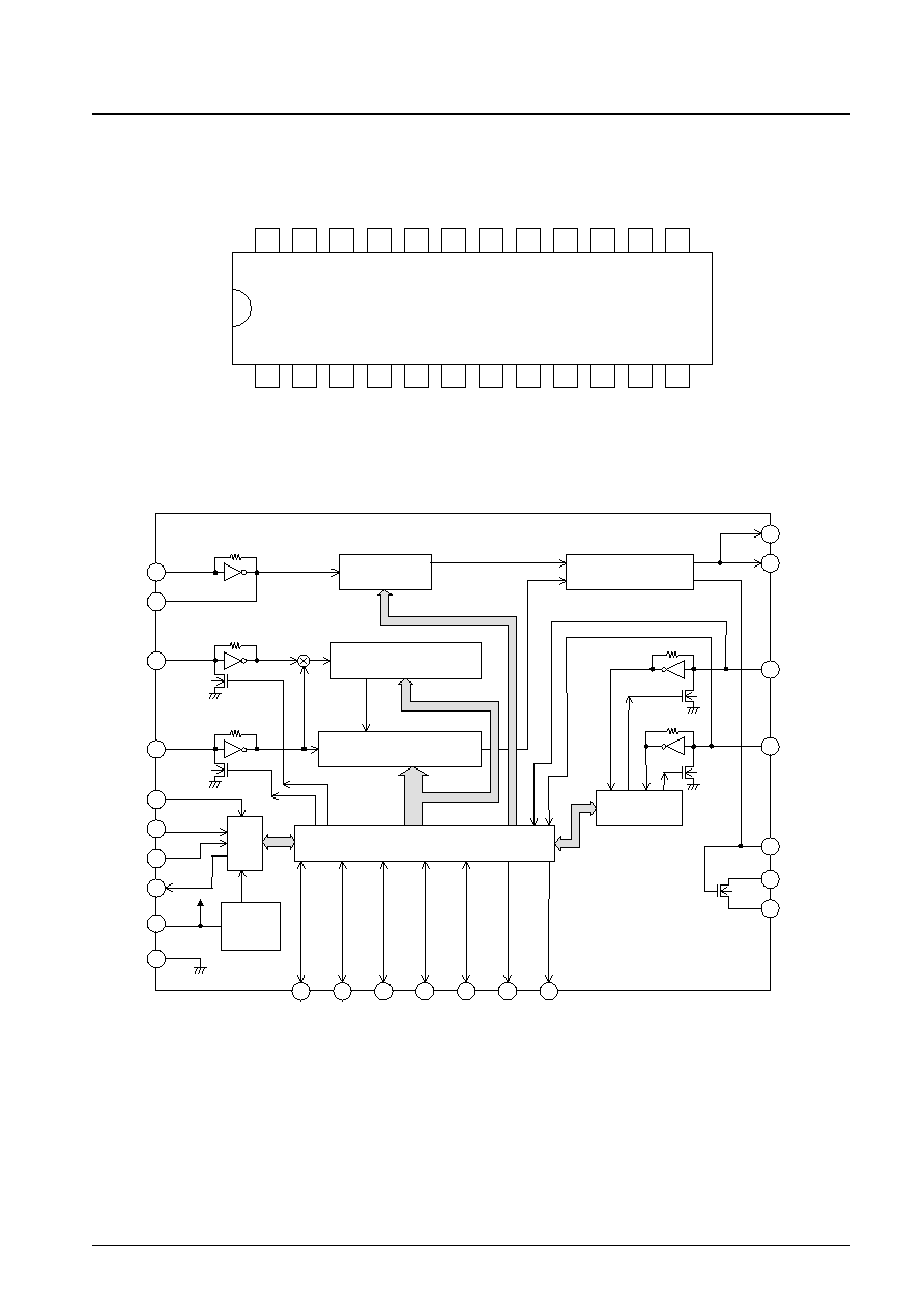
Pin Assignment
No. 6974-2/21
LC72148V
XIN
24
V
SSa
23
A
OUT
22
AIN
21
PD0
20
PD1
19
V
SSd
18
FMIN
17
AMIN
16
V
DD
15
HCTR/I-6
14
LCTR/I-7
13
XOUT
1
CE
2
DI
3
CL
4
DO
5
O-7
6
O-6
7
I/O-5
8
I/O-4
9
I/O-3
10
I/O-2
11
I/O-1
12
Block Diagram
XIN 24
XOUT
1
FMIN 17
AMIN
Power on
reset
CCB
I/F
Data shift register latch
12 bits programmable divider
Swallow counter
1/16, 1/17 4 bits
Reference
divider
Phase detector
charge pump
Universal
counter
16
CE
2
DI
3
CL
4
DO
5
V
DD
15
V
SSd
I/O-1
18
V
SSa
23
AOUT
22
AIN
21
LCTR/I-7
13
HCTR/I-6
14
PD0
20
PD1
19
12
I/O-2
11
I/O-3
10
I/O-4
9
I/O-5
8
O-6
7
O-7
6
No. 6974-3/21
LC72148V
Parameter
Symbol
Conditions
Ratings
Unit
Supply voltage
V
DD
max
V
DD
≠0.3 to +7.0
V
V
IN
1 max
CE, CL, DI
≠0.3 to +7.0
V
Maximum input voltage
V
IN
2 max
XIN, FMIN, AMIN, HCTR/I-6, LCTR/I-7, AIN, I/O-4, I/O-5
≠0.3 to V
DD
+ 0.3
V
V
IN
3 max
I/O-1, I/O-2, I/O-3
≠0.3 to +15.0
V
V
O
1 max
DO
≠0.3 to +7.0
V
Maximum output voltage
V
O
2 max
XOUT, I/O-4, I/O-5, O-6, PD0, PD1, AIN
≠0.3 to VDD + 0.3
V
V
O
3 max
I/O-1, I/O-2, I/O-3, AOUT, O-7
≠0.3 to +15.0
V
I
O
1 max
I/O-4, I/O-5, O-6, O-7
0 to 3.0
mA
Maximum output current
I
O
2 max
DO, AOUT
0 to 6.0
mA
I
O
3 max
I/O-1, I/O-2, I/O-3
0 to 10
mA
Allowable power dissipation
Pd max
(Ta
85∞C) SSOP24
140
mW
Operating temperature
Topr
≠40 to +85
∞C
Storage temperature
Tstg
≠55 to +125
∞C
Specifications
Absolute Maximum Ratings
at Ta = 25∞C, Vssd = Vssa = 0 V
Parameter
Symbol
Conditions
Ratings
Unit
min
typ
max
Supply voltage
V
DD
1
V
DD
2.7
3.6
V
V
DD
2
V
DD
: Serial data retained
1.5
V
V
IH
1
CE, CL, DI, I/O-1, I/O-2, I/O-3
0.7 V
DD
6.5
V
High-level input voltage
V
IH
2
I/O-4, I/O-5, HCTR/I-6, LCTR/I-7
0.7 V
DD
V
DD
V
V
IH
3
LCTR/I-7: Pulse waveform
0.7 V
DD
V
DD
V
Low-level input voltage
V
IL
1
CE, CL, DI, I/O-1 to I/O-5,
0
0.3 V
DD
V
HCTR/I-6, LCTR/I-7
V
IL
2
LCTR/I-7: Pulse waveform
0
0.3 V
DD
V
Output voltage
V
O
1
DO
0
6.5
V
V
O
2
I/O-1, I/O-2, I/O-3, O-7, AOUT
0
13
V
f
IN
1
XIN: V
IN
1
*
1
1
8
MHz
f
IN
2
FMIN: V
IN
2
*
1
10
180
MHz
f
IN
3
AMIN (SNS = 1): V
IN
3
*
1
2
40
MHz
Input frequency
f
IN
4
AMIN (SNS = 0): V
IN
4
*
1
0.5
10
MHz
f
IN
5
HCTR/I-6: V
IN
5
*
1
0.4
25
MHz
f
IN
6
LCTR/I-7: V
IN
6
*
1
10
500
kHz
f
IN
7
LCTR/I-7
*
2
1.0
20
◊
10
3
Hz
V
IN
1
XIN: f
IN
1
200
900
mVrms
V
IN
2-1
FMIN: f = 10 to 130 MHz
20
900
mVrms
V
IN
2-2
FMIN: f = 130 to 180 MHz
40
900
mVrms
V
IN
3
AMIN (SNS = 1): f
IN
3
40
900
mVrms
Input amplitude
V
IN
4
AMIN (SNS = 0): f
IN
4
40
900
mVrms
V
IN
5-1
HCTR/I-3 (CTC = 0): f = 0.4 to 25 MHz
40
900
mVrms
V
IN
5-2
HCTR/I-3 (CTC = 1): f = 8 to 12 MHz
70
900
mVrms
V
IN
6-1
LCTR/I-4 (CTC = 0): f = 10 to 400 kHz
40
900
mVrms
V
IN
6-2
LCTR/I-4 (CTC = 0): f = 400 to 500 kHz
20
900
mVrms
VIN6-3
LCTR/I-4 (CTC = 1): f = 400 to 500 kHz
70
900
mVrms
Guaranteed operation range for
X'tal
XIN, XOUT
*
3
4.0
8.0
MHz
crystal resonator
Allowable Operating Conditions
at Ta = 25∞C, Vssd = Vssa = 0 V
Notes:
1. Sine wave, capacitance coupling
2. Pulse waveform, DC coupling (period measurement)
3. Recommended CI values for the crystal resonator: CI
120
(4.5 MHz) or CI
70
(7.2 MHz)
No. 6974-4/21
LC72148V
Parameter
Symbol
Conditions
Ratings
Unit
min
typ
max
Rf1
XIN
1
M
Rf2
FMIN
500
k
Internal feedback resistors
Rf3
AMIN
500
k
Rf4
HCTR/I-6
250
k
Rf5
LCTR/I-7
250
k
Internal pull-down resistors
Rpd1
FMIN
80
200
600
k
Rpd2
AMIN
80
200
600
k
Hysteresis
V
HIS
CE, CL, DI, LCTR/I-7
0.1 V
DD
V
High-level output voltage
V
OH
1
PD0, PD1, I/O-4, I/O-5, O-6, I
O
= ≠0.5 mA
V
DD
≠ 0.5
V
PD0, PD1, I/O-4, I/O-5, O-6, I
O
= ≠1 mA
V
DD
≠ 1.0
V
V
OH
2
AIN, I
O
= ≠5 mA
V
DD
≠ 1.0
V
V
OL
1
PD0, PD1, I/O-4, I/O-5, O-6, O-7, I
O
= 0.5 mA
0.5
V
PD0, PD1, I/O-4, I/O-5, O-6, O-7, I
O
= 1.0 mA
1.0
V
V
OL
2
AIN, I
O
= 5 mA
1.0
V
I/O-1, I/O-2, I/O-3, I
O
= 1 mA
0.2
V
Low-level output voltage
V
OL
3
I/O-1, I/O-2, I/O-3, I
O
= 2.5 mA
0.5
V
I/O-1, I/O-2, I/O-3, I
O
= 5 mA
1.0
V
I/O-1, I/O-2, I/O-3, I
O
= 9 mA
1.8
V
V
OL
4
DO, I
O
= 5 mA
1.0
V
V
OL
5
AOUT, I
O
= 10 mA, AIN = 2.0 V
1.5
V
I
IH
1
CE, CL, DI, V
I
= 6.5 V
5.0
µA
I
IH
2
I/O-1, I/O-2, I/O-3, V
I
= 13 V
5.0
µA
High-level input current
I
IH
3
I/O-4, I/O-5, HCTR/I-6, LCTR/I-7, V
I
= V
DD
5.0
µA
I
IH
4
XIN, V
I
= V
DD
1.3
8
µA
I
IH
5
FMIN, AMIN, V
I
= V
DD
2.5
15
µA
I
IH
6
HCTR/I-6, LCTR/I-7, V
I
= V
DD
5.0
30
µA
I
IL
1
CE, CL, DI, V
I
= 0 V
5.0
µA
I
IL
2
I/O-1, I/O-2, I/O-3, V
I
= 0 V
5.0
µA
Low-level input current
I
IL
3
HCTR/I-6, LCTR/I-7, V
I
= 0 V
5.0
µA
I
IL
4
XIN, V
I
= 0 V
1.3
8
µA
I
IL
5
FMIN, AMIN, V
I
= 0 V
2.5
15
µA
I
IL
6
HCTR/I-6, LCTR/I-7, V
I
= 0 V
5.0
30
µA
Output off leakage current
I
OFF
1
I/O-1, I/O-2, I/O-3, O-7, AOUT, V
O
= 13 V
5.0
µA
I
OFF
2
DO, V
O
= 6.5 V
5.0
µA
High-level three-state off leakage
I
OFFH
PD0, PD1, AIN, V
O
= V
DD
0.01
200
nA
current
Low-level three-state off leakage
I
OFFL
PD0, PD1, AIN, V
O
= 0 V
0.01
200
nA
current
Input capacitance
C
IN
FMIN
6
pF
I
DD
1
V
DD
, X'tal = 7.2 MHz, f
IN
2 = 180 MHz, V
IN
2 = 40 mVrms,
3
8
mA
f
IN
5 = 25 MHz, V
IN
5 = 40 mVrms
V
DD
, With the PLL block stopped. (PLL INHIBIT)
Supply current
I
DD
2
With the crystal oscillator operating.
0.5
1.5
mA
(Crystal frequency = 7.2 MHz)
I
DD
3
V
DD
, With the PLL block stopped.
10
µA
With the crystal oscillator stopped.
Electrical Characteristics
for the Allowable Operating Ranges
No. 6974-5/21
LC72148V
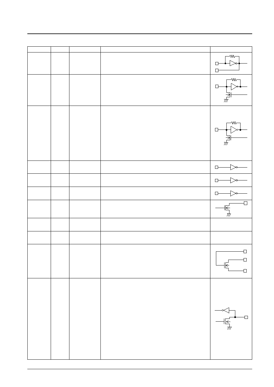
Pin Functions
Pin No.
Symbol
Type
Function
Pin circuit
∑ Crystal resonator connections (7.2 or 4.5 MHz)
XIN
XOUT
24
1
X'tal
∑ FMIN is selected when DVS in the serial data input is set to 1.
∑ The input frequency range is 10 to 180 MHz.
∑ The signal is directly transmitted to the swallow counter.
∑ The divisor can be set to a value in the range 272 to 65,535.
FMIN
17
Local oscillator
signal input
∑ AMIN is selected when DVS in the serial data input is set to 0.
∑ When SNS in the serial data input is set to 1:
-- The input frequency range is 2 to 40 MHz.
-- The signal is directly transmitted to the swallow counter.
-- The divisor can be set to a value in the range 272 to 65,535.
∑ When SNS in the serial data input is set to 0:
-- The input frequency range is 0.5 to 10 MHz.
-- The signal is directly transmitted to the 12-bit programmable divider.
-- The divisor can be set to a value in the range 5 to 4,095.
AMIN
16
Local oscillator
signal input
∑ This pin must be set to the high level during serial data input (DI) from, or
serial data output (DO) to, the LC72148V.
CE
2
S
Chip enable
∑ Input pin for serial data transmitted from the controller to the LC72148V.
DI
3
S
Input data
∑ Data synchronization clock used during serial data input (DI) from, or
serial data output (DO) to, the LC72148V.
CL
4
S
Clock
∑ Data output pin for data output from the LC72148V to the controller.
The content of the data output is determined by the ULD, DT0, and DT1
bits in the serial data.
DO
5
Output data
∑ The LC72148V power supply pin. (V
DD
= 2.7 to 3.6 V)
∑ The power-on reset circuit operates when power is first applied.
------
------
V
DD
15
Power supply
∑ Digital system ground for the LC72148V
V
SSd
18
Ground
∑ Connections to the internal n-channel MOS transistor provided to
implement an active low-pass filter for the PLL.
∑ A high-speed locking circuit can be implemented by using these pins in
conjunction with the built-in sub-charge pump.
∑ See the item describing the structure of the charge pump for details.
∑ Vssa is a dedicated ground pin.
AIN
AOUT
V
SSa
21
22
23
Low-pass filter
amplifier transistor
∑ Input/output shared-function pins
∑ In output mode, the circuits are open-drain outputs.
∑ The I/O direction is determined by I/O-1 to I/O-3 in the serial data.
When the data is 0: input port
When 1: output port
∑ When specified for use as input ports
The input pin states are transmitted from the DO pin to the controller
Input state = low : Data = 0
Input state = high : Data = 1
∑ When specified for use as output ports
The output states are determined by OUT1 to OUT3 in the serial data.
Data = 0 : low
Data = 1 : open
∑ These pins are set to function as input ports by the power-on reset.
I/O-1
I/O-2
I/O-3
12
11
10
General-purpose
I/O ports
Continued on next page.