 | –≠–ª–µ–∫—Ç—Ä–æ–Ω–Ω—ã–π –∫–æ–º–ø–æ–Ω–µ–Ω—Ç: LC7218JM | –°–∫–∞—á–∞—Ç—å:  PDF PDF  ZIP ZIP |
CMOS LSI
Ordering number : EN4758B
63096HA (OT)/42895TH (OT) No. 4758-1/16
SANYO Electric Co.,Ltd. Semiconductor Bussiness Headquarters
TOKYO OFFICE Tokyo Bldg., 1-10, 1 Chome, Ueno, Taito-ku, TOKYO, 110 JAPAN
PLL Frequency Synthesizer
for Electronic Tuning in AV Systems
LC7218, 7218M, 7218JM
Overview
The LC7218, LC7218M and LC7218JM are PLL
frequency synthesizers for electronic tuning. The LC7218,
LC7218M and LC7218JM are optimal for AM/FM tuner
circuits that require high mounting densities.
Features
∑ These products feature a rich set of built-in functions for
AV applications, including reference frequency and
unlock detection circuits, I/O ports and a general-
purpose counter.
Functions
∑ Programmable dividers
-- FMIN pin: 130 MHz at 70 mVrms and 160 MHz at
100 mVrms input (built-in prescaler)
-- AMIN pin: Pulse swallower and direct division
techniques
∑ Reference frequencies: Ten selectable frequencies:
1, 5, 9, 10, 3.125, 6.25, 12.5 25, 50 and 100 kHz
∑ Output ports: 7 pins
Complementary outputs: 2 pins
N-channel open drain outputs: 5 pins
∑ Input ports: 2 pins
∑ General-purpose counter: For measuring IF and other
signals (Also used for station detection when
functioning as an IF counter.)
-- HCTR pin: Frequency measurement (for inputs up
to 70 MHz)
-- LCTR pin: Frequency and period measurement
∑ PLL unlock detection circuit
Detects phase differences of 0.55, 1.11, 2.22 and 3.33 µs.
∑ Controller clock output: 400 kHz
∑ Clock time base output: 8 Hz
∑ Serial data I/O
-- Supports CCB format communication with the
system controller.
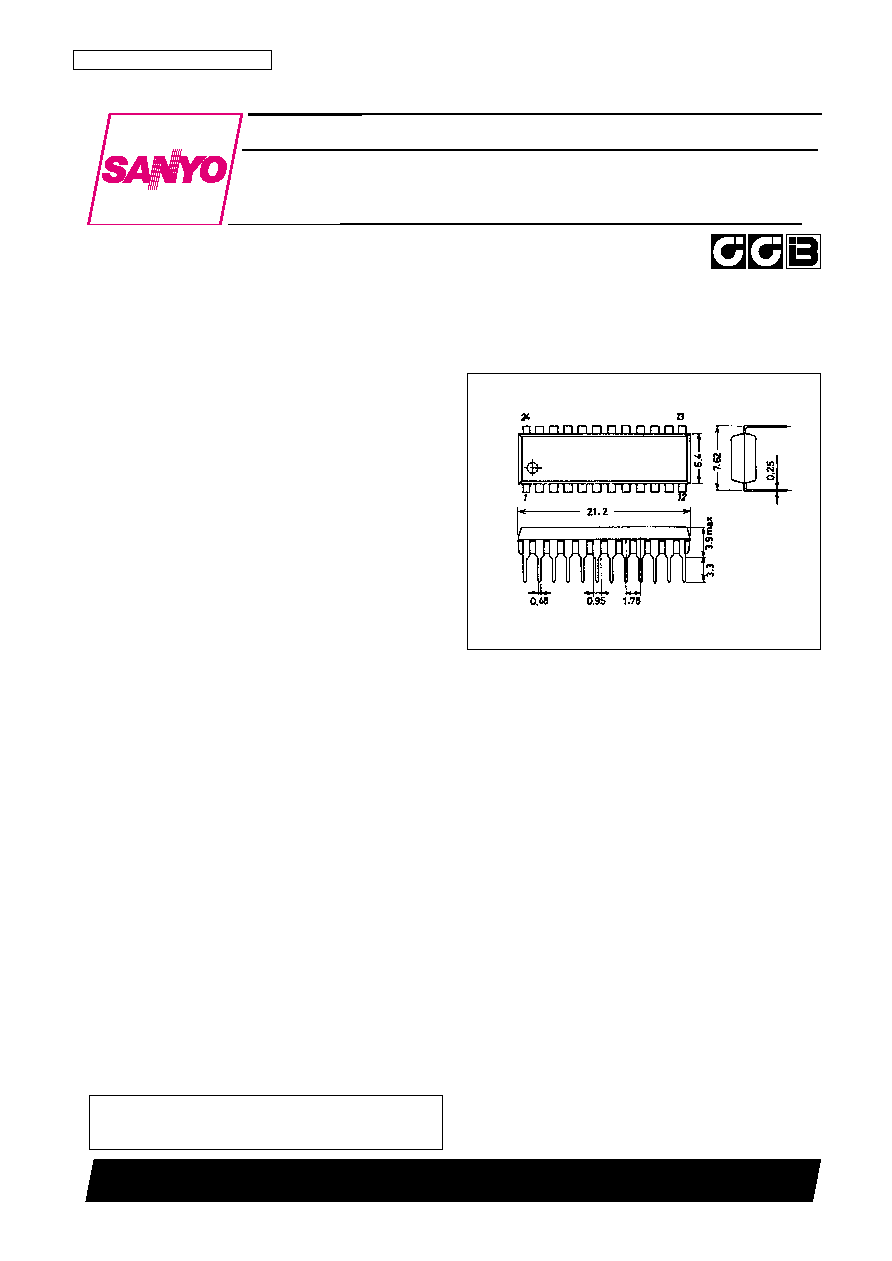
∑ Package: LC7218: DIP24S
LC7218M: MFP24
LC7218JM: MFP24S
Package Dimensions
unit: mm
3067-DIP24S
SANYO: DIP24S
[LC7218]
∑ CCB is a trademark of SANYO ELECTRIC CO., LTD.
∑ CCB is SANYO's original bus format and all the bus
addresses are controlled by SANYO.
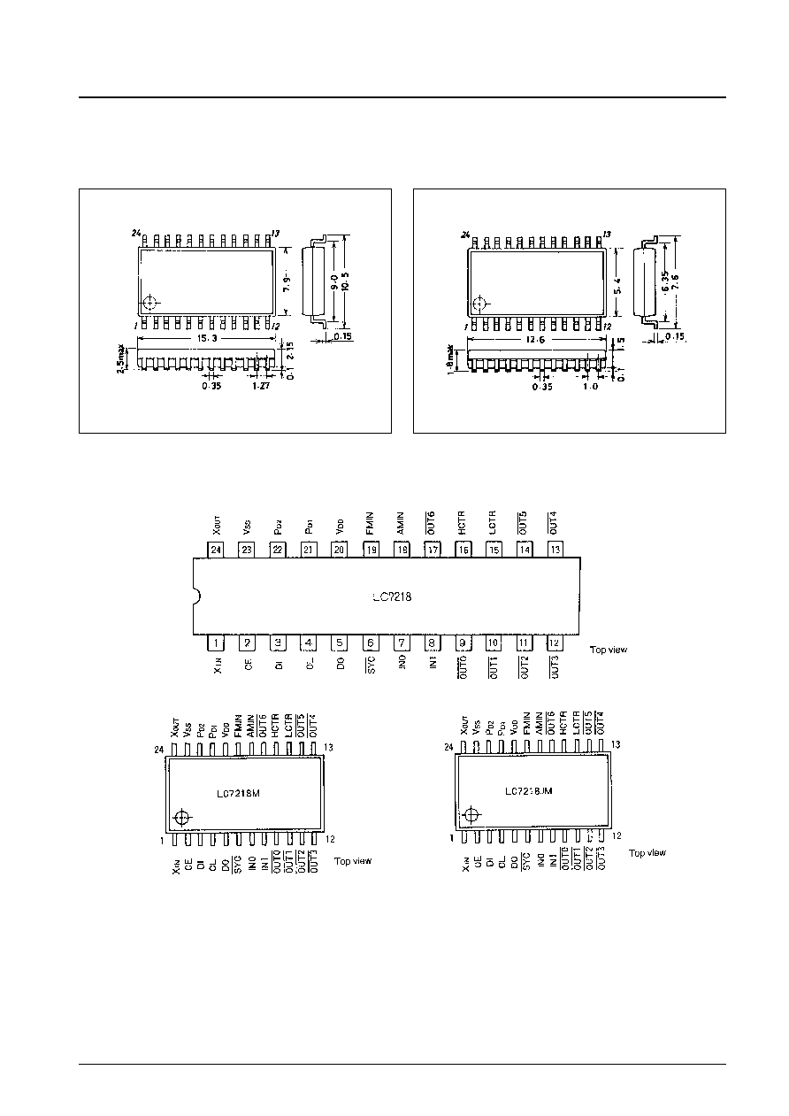
Package Dimensions
unit: mm
unit: mm
3045B-MFP24
3112-MFP24S
Pin Assignments
No. 4758-2/16
LC7218, 7218M, 7218JM
SANYO: MFP24
[LC7218M]
SANYO: MFP24S
[LC7218JM]
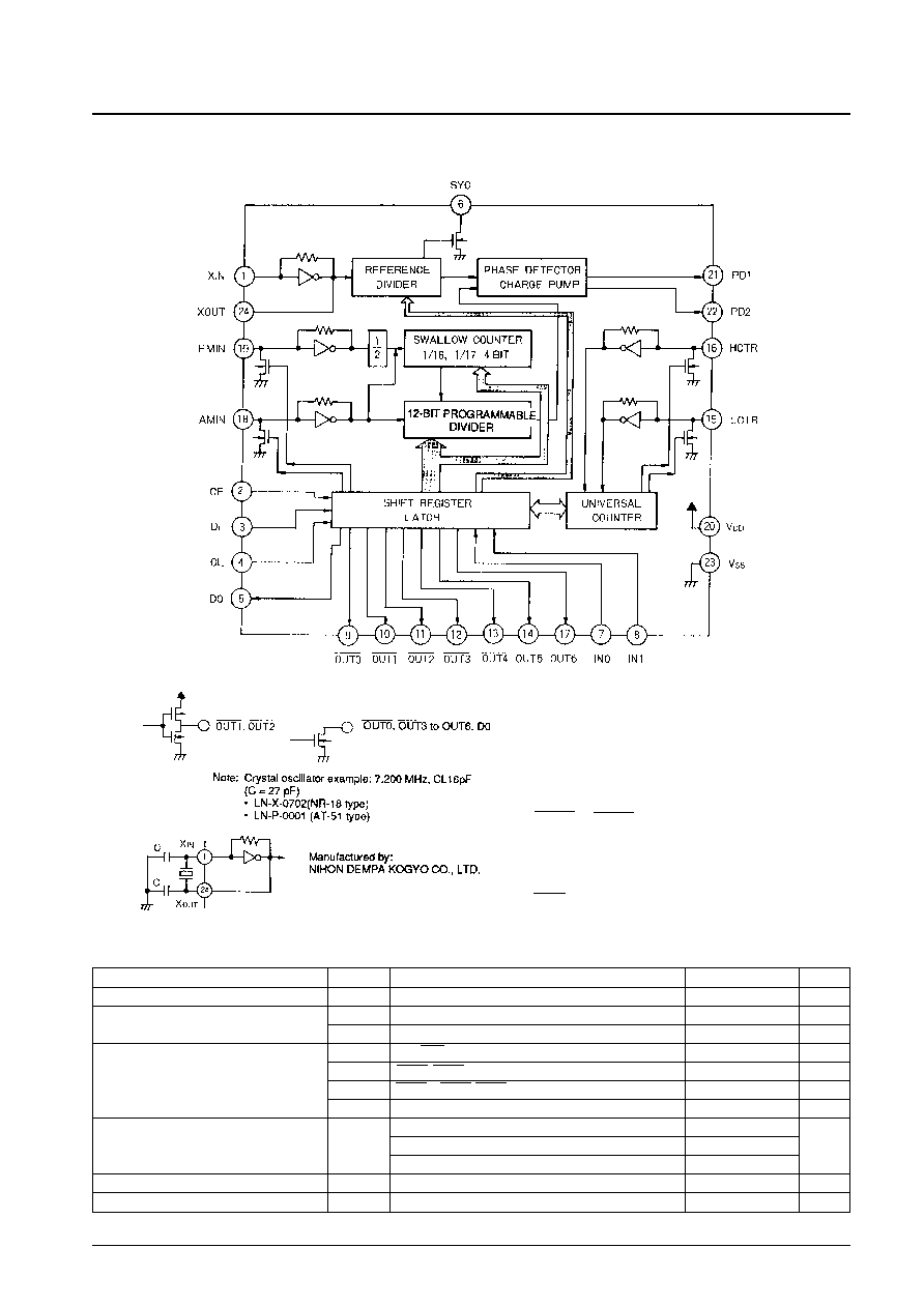
Block Diagram
Pin Symbols
XIN, XOUT:
Crystal oscillator (7.2 MHz)
FMIN, AMIN:
Local oscillator signal input
CE, CL, DI, DO: Serial data I/O
OUT0 to OUT6: Output ports
IN0, IN1:
Input ports
HCTR, LCTR:
General-purpose counter inputs
PD1, PD2:
Charge pump outputs
SYC:
Control clock (400 kHz)
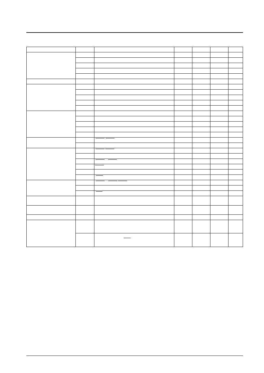
Specifications
Absolute Maximum Ratings
at Ta = 25∞C, V
SS
= 0 V
No. 4758-3/16
LC7218, 7218M, 7218JM
Parameter
Symbol
Conditions
Ratings
Unit
Maximum supply voltage
V
DD
max
V
DD
≠0.3 to +7.0
V
Input voltage
V
IN
(1)
CE, CL, DI, IN0, IN1
≠0.3 to +7.0
V
V
IN
(2)
Input pins other than V
IN
(1)
≠0.3 to V
DD
+ 0.3
V
V
OUT
(1)
DO, SYC
≠0.3 to +7.0
V
Output voltage
V
OUT
(2)
OUT1, OUT2
≠0.3 to V
DD
+ 0.3
V
V
OUT
(3)
OUT3 to OUT6, OUT0
≠0.3 to +15
V
V
OUT
(4)
Output pins other than V
OUT
(1), V
OUT
(2) and V
OUT
(3)
≠0.3 to V
DD
+ 0.3
V
Ta
85∞C
:LC7218
350
Allowable power dissipation
Pd max
:LC7218M
300
mW
:LC7218JM
200
Operating temperature
Topr
≠40 to +85
∞C
Storage temperature
Tstg
≠55 to +125
∞C
Allowable Operating Ranges
at Ta = ≠40 to +85∞C, V
SS
= 0 V
Note: 1.
DV and SP are bits in the serial data.
*
: don't care
2. Frequency measurement
3. Frequency measurement
4. Period measurement
5. f
IN
(2): 10 to 160 MHz/V
IN
(2)
0.100 Vrms (minimum)
6. f
IN
(4): 10 to 70 MHz/V
IN
(4)
0.100 Vrms (minimum)
No. 4758-4/16
LC7218, 7218M, 7218JM
Parameter
Symbol
Conditions
min
typ
max
Unit
Supply voltage
V
DD
(1)
V
DD
4.5
6.5
V
V
DD
(2)
V
DD
: Crystal oscillator guaranteed operation
3.5
6.5
V
Input high level voltage
V
IH
(1)
CE, CL, DI, IN0, IN1
2.2
6.5
V
V
IH
(2)
LCTR: Pulse waveform, DC coupling
*
4
0.7 V
DD
(1)
V
DD
(1)
V
Input low level voltage
V
IL
(1)
CE, CL, DI, IN0, IN1
0
0.7
V
V
IL
(2)
LCTR
*
4
0
0.3 V
DD
(1)
V
Output voltage
V
OUT
(1)
DO, SYC
6.5
V
V
OUT
(2)
OUT3 to OUT6, OUT0
13
V
f
IN
(1)
XIN: Sine wave capacitor coupling, V
DD
(2)
1.0
7.2
8.0
MHz
f
IN
(2)
FMIN: Sine wave capacitor coupling, V
DD
(1)
*
1
10
130 (160)
*
5
MHz
Input frequency
f
IN
(3)
AMIN: Sine wave capacitor coupling, V
DD
(1)
*
1
0.5
40
MHz
f
IN
(4)
HCTR: Sine wave capacitor coupling, V
DD
(1)
*
2
10
60 (70)
*
6
MHz
f
IN
(5)
LCTR: Sine wave capacitor coupling, V
DD
(1)
*
3
15
500
kHz
f
IN
(6)
LCTR: Pulse wave DC coupling, V
DD
(1)
*
4
1.0
20
◊
10
3
Hz
Crystal oscillators for which
Xtal
X
IN
-X
OUT
: CI
50
3.0
7.2
8.0
MHz
operation is guaranteed
V
IN
(1)
X
IN
: Sine wave capacitor coupling, V
DD
(1)
0.5
1.5
Vrms
V
IN
(2)
FMIN: Sine wave capacitor coupling, V
DD
(1)
0.070
1.5
Vrms
(0.100)
*
5
Input amplitude
V
IN
(3)
AMIN: Sine wave capacitor coupling, V
DD
(1)
0.070
1.5
Vrms
V
IN
(4)
HCTR: Sine wave capacitor coupling, V
DD
(1)
*
2
0.070
1.5
Vrms
(0.100)
*
6
V
IN
(5)
LCTR: Sine wave capacitor coupling, V
DD
(1)
*
3
0.070
1.5
Vrms
DV
SP
Input frequency
1/2 divider
1/16, 17 swallow
12-bit main divider
Input pin
1
*
10 to 130 (160) MHz
q
q
q
q
q
q
FMIN
0
1
2 to 40 MHz
--
q
q
q
q
AMIN
0
0
0.5 to 10 MHz
--
--
q
q
AMIN
Electrical Characteristics
for the Allowable Operating Ranges
Note: A capacitor of at least 2000 pF must be inserted between the power supply V
DD
and V
SS
potentials.
No. 4758-5/16
LC7218, 7218M, 7218JM
Parameter
Symbol
Conditions
min
typ
max
Unit
Rf (1)
XIN
1.0
M
Rf (2)
FMIN
500
k
Internal feedback resistance
Rf (3)
AMIN
500
k
Rf (4)
HCTR
500
k
Rf (5)
LCTR
500
k
Hysteresis
V
H
LCTR
0.1 V
DD
0.6 V
DD
V
I
IH
(1)
CE, CL, DI: V
I
= 6.5 V
5.0
µA
I
IH
(2)
IN0, IN1: V
I
= V
DD
5.0
µA
Input high level current
I
IH
(3)
XIN: V
I
= V
DD
20
µA
I
IH
(4)
FMIN, AMIN: V
I
= V
DD
40
µA
I
IH
(5)
HCTR, LCTR: V
I
= V
DD
40
µA
I
IL
(1)
CE, CL, DI: V
I
= V
SS
5.0
µA
I
IL
(2)
IN0, IN1: V
I
= V
SS
5.0
µA
Input low level current
I
IL
(3)
XIN: V
I
= V
SS
20
µA
I
IL
(4)
FMIN, AMIN: V
I
= V
SS
40
µA
I
IL
(5)
HCTR, LCTR: V
I
= V
SS
40
µA
Output high level voltage
V
OH
(1)
OUT1, OUT2: I
O
= ≠1 mA
V
DD
≠ 1.0
V
V
OH
(2)
PD1, PD2: I
O
= ≠0.5 mA
V
DD
≠ 1.0
V
V
OL
(1)
OUT1, OUT2: I
O
= 1 mA
1.0
V
V
OL
(2)
PD1, PD2: I
O
= 0.5 mA
1.0
V
Output low level voltage
V
OL
(3)
OUT3 to OUT6: I
O
= 5 mA
1.0
V
V
OL
(4)
OUT0: I
O
= 1 mA
1.0
V
V
OL
(5)
DO: I
O
= 5 mA
1.0
V
V
OL
(6)
SYC: I
O
= 0.5 mA (V
DD
= 3.5 to 6.5 V)
1.0
V
I
OFF
(1)
OUT3 to OUT6, OUT0: V
O
= 13 V
5.0
µA
Output off leakage current
I
OFF
(2)
DO: V
O
= 6.5 V
5.0
µA
I
OFF
(3)
SYC: V
O
= 6.5 V (V
DD
= 3.5 to 6.5 V)
5.0
µA
Three-state high level
I
OFFH
PD1, PD2: V
O
= V
DD
0.01
10.0
nA
off leakage current
Three-state low level
I
OFFL
PD1, PD2: V
O
= V
SS
0.01
10.0
nA
off leakage current
Input capacitance
C
IN
FMIN, HCTR
1
2
3
pF
V
DD
: f
IN
(2) = 130 MHz, V
IN
(2) = 70 mVrms,
I
DD
(1)
with a 7.2 MHz crystal, other input pins at V
SS
,
20
30
mA
Current drain
output pins open
V
DD
: PLL block stopped (PLL inhibit state), crystal
I
DD
(2)
oscillator operating (SYC, TB), with a 7.2 MHz crystal,
1.0
mA
other input pins at V
SS
, output pins open
Pin Functions
Note:
*
The high and low level input voltages for the CE, CL, DI, IN0 and IN1 pins are V
IH
= 2.2 to 6.5 V and V
IL
= 0 to 0.7 V, regardless of the power
supply voltage V
DD
.
No. 4758-6/16
LC7218, 7218M, 7218JM
Pin No.
Symbol
I/O
Type
Function
1
24
19
18
21
22
6
20
23
2
4
3
5
X
IN
X
OUT
FMIN
AMIN
PD1
PD2
SYC
V
DD
V
SS
CE
CL
DI
DO
Input
Output
Input
Input
Three-state
N-channel
open drain
--
--
Input
*
Input
*
Input
*
Output
(N-channel
open drain)
Xtal OSC
Local oscillator signal
input
Local oscillator signal
input
Charge pump outputs
Controller clock
Power supply
Ground
Chip enable
Clock
Input data
Output data
∑ Connections for a 7.2 MHz crystal oscillator
∑ FMIN is selected when DV in the serial input data is set to 1.
∑ Input frequency range: 10 to 130 MHz (70 mVrms minimum)
∑ The signal passes through an internal divide-by-two prescaler and is then supplied to
the swallow counter.
∑ Although the divisor setting is in the range 256 to 65,536, the actual divisor will be twice
the set value due to the presence of the internal divide-by-two prescaler.
∑ AMIN is selected when DV in the serial input data is set to 0.
∑ When SP in the serial input data is set to 1:
-- Input frequency range: 2 to 40 MHz (70 mVrms minimum).
-- The signal is supplied directly to the swallow counter without passing through the
internal divide-by-two prescaler.
-- The divisor setting is in the range 256 to 65,536 and the actual divisor will be the
value set.
∑ When SP in the serial input data is set to 0:
-- Input frequency range: 0.5 to 10 MHz (70 mVrms minimum).
-- The signal is supplied directly to a 12-bit programmable divider.
-- The divisor setting is in the range 4 to 4,096 and the actual divisor will be the
value set.
∑ PLL charge pump outputs. High levels are output from PD1 and PD2 when the local
oscillator frequency divided by n is higher than the reference frequency, and low levels
are output when that frequency is lower than the reference frequency.
These pins go to the floating state when the frequencies agree.
∑ SYC is a controller clock source. The LC7218 outputs a 400 kHz 66% duty signal
from this pin after power is applied.
∑ The LC7218 power supply pin. A voltage of between 4.5 and 6.5 V must be provided
when the PLL is operating. The supply voltage can be lowered to 3.5 V when only
operating the crystal oscillator circuit to acquire the controller clock and the clock time
base outputs.
∑ The LC7218 ground pin
∑ This pin must be set high when inputting serial data (via DI) or when outputting serial
data (via DO).
∑ The clock input used for data signal synchronization during serial data input (via DI) or
output (via DO).
∑ Input pin used when transferring serial data from the controller to the LC7218.
∑ A total of 36 bits of data must be supplied to set up the LC7218 initial state.
∑ Output pin used when transferring serial data to the controller from the LC7218.
∑ A total of 28 bits from an internal shift register can be output in synchronization with the
CL signal.
Continued on next page.
Continued from preceding page.
Note:
*
1. Since the output port states are undefined when power is first applied, transfer the control data quickly.
*
2. The high and low level input voltages for the CE, CL, DI, IN0 and IN1 pins are V
IH
= 2.2 to 6.5 V and V
IL
= 0 to 0.7 V, regardless of the power
supply voltage V
DD
.
Control Data Format (serial input data)
No. 4758-7/16
LC7218, 7218M, 7218JM
Pin No.
Symbol
I/O
Type
Function
9
10
11
12
13
14
17
7
8
16
15
OUT0
OUT1
OUT2
OUT3
OUT4
OUT5
OUT6
IN0
IN1
HCTR
LCTR
Output
*
1
Input
*
2
Input
Input
Output port
Input port
General-purpose
counter
Frequency
measurement signal
input pin
General-purpose
counter
Frequency or period
measurement signal
input pin
∑ These pins latch bits O
0
to O
6
in the serial data transferred from the controller, invert
that data and output the inverted data in parallel.
∑ The OUT0 pin can also be used to output an 8 Hz clock time base signal.
(When TB is 1.)
∑ OUT1 and OUT2 are complementary outputs.
∑ OUT0, OUT3, OUT4, OUT5 and OUT6 are N-channel open drain outputs that can
handle up to 13 V.
∑ The values of the IN0 and IN1 input ports can be converted from parallel to serial and
output from the DO output pin.
∑ HCTR is selected when SC in the serial input data is set to 1.
∑ Input frequency range: 10 to 60 MHz (70 mVrms minimum)
∑ The signal is supplied to a general-purpose 20-bit binary counter after passing through a
divide-by-eight circuit. Therefore, the value of the counter is 1/8 of the frequency actually
input to HCTR.
∑ When HCTR is selected the LC7218 will function in frequency measurement mode
and the measurement period can be selected to be either 60 or 120 ms. (GT = 0: 60 ms,
1: 120 ms)
∑ The result of the measurement (the value of the general-purpose counter) can be output
MSB first from the DO output pin.
∑ LCTR is selected when SC in the serial input data is set to 0.
∑ When SF in the serial input data is set to 1:
-- Frequency measurement mode is selected.
-- Input frequency range: 15 to 500 kHz (70 mVrms minimum).
-- The signal is supplied directly to the general-purpose counter without passing
through the internal divide-by-eight circuit.
-- The measurement period is the same as for HCTR.
∑ When SF in the serial input data is set to 0:
-- Period measurement mode is selected.
-- Input frequency range: 1 Hz to 20 kHz (V
IH
= 0.7 V
DD
minimum, V
IL
= 0.3∑V
DD
maximum)
-- The measurement can be selected to be for one or two cycles. If two cycle
measurement is selected the input frequency range becomes 2 Hz to 20 kHz.
(GT = 0: one cycle, 1: two cycles)
∑ Measurement results are output in the same manner as HCTR measurement results.
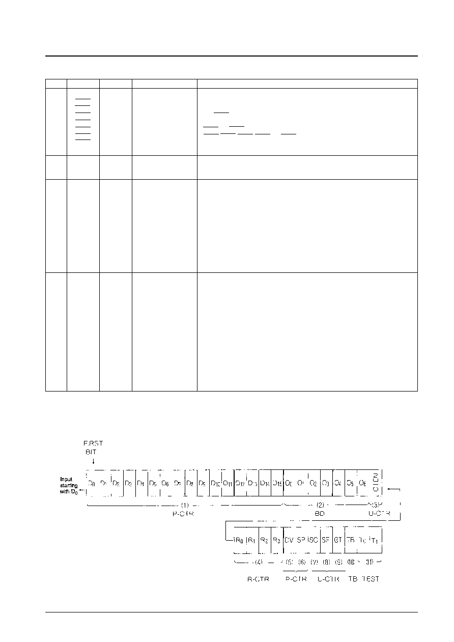
The LC7218 control data consists of 36 bits. All 36 bits must be input after power is applied to set up the LC7218 initial
state. This is because the last two bits, while being unrelated to user functions, are data that switches the LSI test modes.
Once the LC7218 has been initialized, the contents of the first 24 bits (D
0
to CTEN) can be changed without changing
the contents of the last 12 bits (R0 to T1) by inputting data to DI in serial data input mode.
No. 4758-8/16
LC7218, 7218M, 7218JM
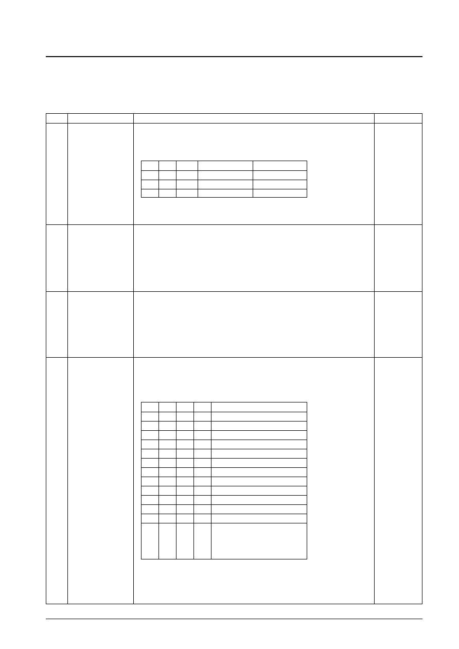
No.
Control block/data
Description
Related data
(1)
(2)
(3)
(4)
Programmable divider
data
D
0
to D
15
Output port data
O
0
to O
6
General-purpose counter
initial data
CTEN
Reference frequency
data
R
0
to R
3
∑ This data sets up the programmable divider.
D
0
to D
15
is a binary value with D
15
as the MSB.
The position of the LSB is changed by DV and SP as listed in the table below.
*
don't care
When D
4
is the LSB, bits D
0
to D
3
are ignored.
∑ Data that determines the states of the output ports OUT0 to OUT6. O
0
determines the
OUT0 pin output. However, note that when O
0
is 0, OUT0 will output a high level, and when O
0
is 1, OUT0 will output a low level. O
1
to O
6
function in the same manner.
∑ These can be used for a wide range of purposes, including, for example, band switching
signals.
∑ When the TB bit is set to 1, the O
0
data is ignored and the OUT0 pin outputs an 8 Hz clock
time base signal.
∑ Since the output port states are undefined when power is first applied, transfer the control data
quickly.
∑ Data that determines the operation of the general-purpose counter. When CTEN is 0, the 20-bit
binary counter (the general-purpose counter) is reset and the HCTR and LCTR pins are pulled
down to ground. When CTEN is set to 1, the general-purpose counter reset state is cleared and
the counter operates according to the SC bit (the general-purpose selection data). In this state,
the general-purpose counter will count either the HCTR or LCTR input signal.
∑ Since the general-purpose counter is reset by setting CTEN to 0, the result of a count operation
must be sent to the controller while CTEN is still 1.
∑ Data that selects one of the ten LC7218 reference frequencies or sets the LC7218 to
backup mode in which PLL operation is disabled.
Note:
*
PLL inhibit (backup mode)
The programmable divider block is turned off, both the FMIN and AMIN pins are pulled
down to ground, and the charge pump outputs go to the floating state.
DV
SP
TB
SC
SF
GT
DV
SP
LSB
Divisor setting
Actual divisor
1
*
D0
256 to 65536
Twice the set value
0
1
D0
256 to 65536
The set value
0
0
D4
4 to 4096
The set value
R
0
R
1
R
2
R
3
Reference frequency (kHz)
0
0
0
0
100
0
0
0
1
50
0
0
1
0
25
0
0
1
1
25
0
1
0
0
12.5
0
1
0
1
6.25
0
1
1
0
3.125
0
1
1
1
3.125
1
0
0
0
10
1
0
0
1
9
1
0
1
0
5
1
0
1
1
1
1
1
0
0
1
1
0
1
PLL inhibit state
*
1
1
1
0
1
1
1
1
Continued on next page.
Continued from preceding page.
DO Output Format (serial data output)
The LC7218 includes a 28-bit internal shift register that can be used to output the following data from DO: the IN0 and
IN1 input port states, the general-purpose counter (20-bit binary counter) and the unlock detection circuit state.
The contents of the shift register is latched at the point that serial data output mode is selected.
No. 4758-9/16
LC7218, 7218M, 7218JM
No.
Control block/data
Description
Related data
(5)
(6)
(7)
(8)
(9)
(10)
(11)
Divider selection data
DV
Sensitivity selection
data
SP
General-purpose
counter input pin
selection data
SC
General-purpose
counter
frequency/period mode
switching data
SF
General-purpose
counter count time
selection data
GT
Time base output
control data
TB
LSI test mode control
data
T
0
, T
1
∑ DV selects the local oscillator input pin. (FMIN or AMIN)
∑ SP switches the input frequency range when AMIN is selected.
*
don't care
∑ SC selects the input pin (HCTR or LCTR) for the general-purpose counter.
∑ SF selects the measurement type (frequency or period) when LCTR is selected.
When HCTR is selected, SF is ignored and the LC7218 operates in frequency measurement
mode.
*
don't care
∑ GT selects the measurement time in frequency measurement mode and the number of periods
in period measurement mode.
GT = 0: 60 ms/one period
GT = 1: 120 ms/two periods
(frequency measurement/period measurement)
∑ When TB is set to 1 an 8 Hz 40% duty clock time base signal is output from OUT0. O
0
bit is
ignored in this mode.
∑ T
0
and T
1
switch the LSI between test and normal operating modes. The test modes and have
no user related functions. Both T
0
and T
1
must always be set to 0.
Be sure to set both T
0
and T
1
to 0 after power is applied.
CTEN
GT
CTEN
SC
SF
O
0
DV
SP
Input pin
Input frequency range (MHz)
1
*
FMIN
10 to 130
0
1
AMIN
2 to 40
0
0
AMIN
0.5 to 10
DV
SP
Input pin
Measurement type
1
*
HCTR
Frequency measurement (sine wave)
0
1
LCTR
Frequency measurement (sine wave)
0
0
LCTR
Period measurement (pulse waveform)
No.
Data
Description
(1)
Input port data
∑ The values of the IN0 and IN1 input ports are latched into I
0
and I
1
.
I
0
and I
1
I
0
IN
0
, I
1
IN
1
General-purpose
∑ The C
19
to C
0
data is latched from value of the general-purpose 20-bit binary counter.
(2)
counter binary data
C
19
20-bit binary counter MSB
C
19
to C
0
C
0
20-bit binary counter LSB
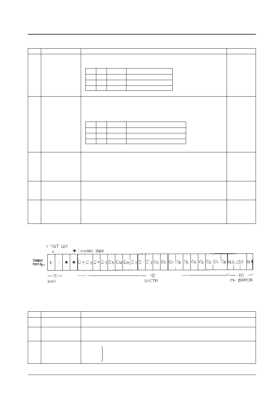
∑ The UL3 to UL0 data is latched from the unlock detection circuit.
PLL unlock state data
UL0: 1.11
(3)
UL3 to UL0
UL1: 2.22
These bits are set to 1 if a phase difference in excess of these times (in µs) was detected.
UL2: 3.33
(for a 7.2 MHz crystal)
UL3: 0.55
Serial Data I/O Methods
The LC7218 supports a total of three I/O modes: two control data input (serial data input) modes and one DO output
(serial data output) mode. Data I/O is performed after the mode has been determined.
The mode is selected by four data items (A
0
to A
3
) synchronized with a clock (the CL pin) applied before the CE pin is
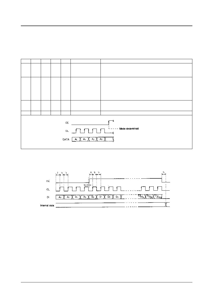
set high. The mode is determined when the CE pin goes high.
1. In the serial data input modes (modes 1 and 2), t
1
1.5 µs, t
2
0 µs, t
3
1.5 µs, and t
4
< 1.5 µs.
∑ Mode 1: A total of 40 bits, the four mode selection bits and the 36 control data bits (from D
0
to T
1
), are input from
the DI pin in synchronization with the clock (CL) signal.
∑ Mode 2: A total of 28 bits, the four mode selection bits and 24 control data bits (from D
0
to CTEN), are input from
the DI pin in synchronization with the clock (CL) signal.
No. 4758-10/16
LC7218, 7218M, 7218JM
Mode
A
3
A
2
A
1
A
0
Item
Function
∑ This mode is used to input all 36 bits of the control data (serial input data).
1
0
0
0
1
Serial data input (all bits)
This mode is used for initialization following power on and to change data that
cannot be changed in mode 2. All 36 bits of the control data is input from the
LC7218 DI pin.
∑ This mode is used to input a subset (24 bits) of the control data (serial input
data).
Serial data input
This mode is used to change three data items: the programmable divider data
2
0
0
1
0
(partial input)
(D
0
to D
15
), the output port data (O
0
to O
6
) and the general-purpose counter
start data (CTEN), for a total of 24 bits. The other 12 bits of control data are not
changed by a mode 2 operation. (Use mode 1 when the other 12 bits must be
changed.)
∑ The DO output mode (serial data output) is used to output three data items from
3
0
0
1
1
Serial data output
the DO pin: the input port data, the general-purpose counter binary data and the
PLL unlock state data.
0 to 0
1 to 0
0 to 0
0 to 0
Invalid setting
∑ This mode is invalid and does not support any data input or output operations.
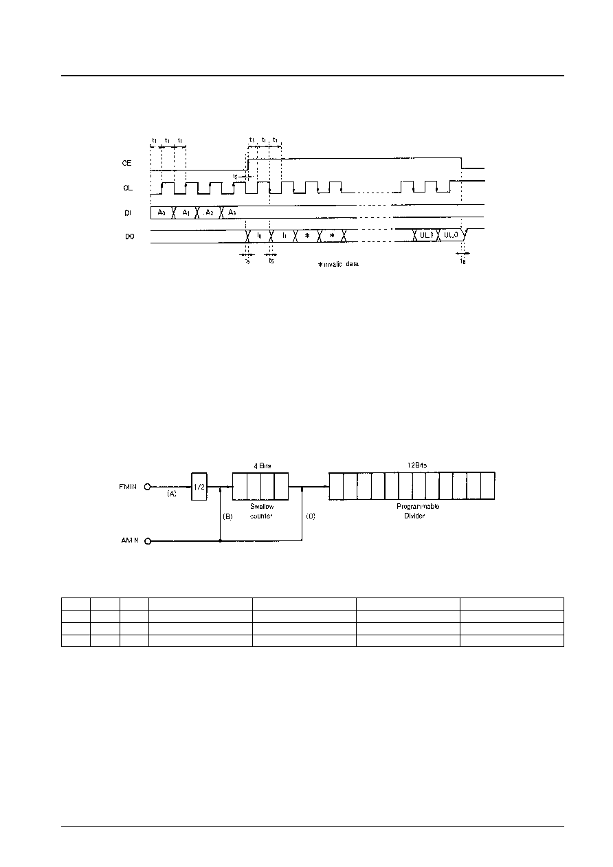
2. In serial data output mode (mode 3), t
1
1.5 µs, t
2
0 µs, t
3
1.5 µs, and t
5
< 1.5 µs. (However, note that since the
DO pin is an n-channel open drain output, the transition time depends on the value of the pull-up resistor.)
∑ Mode 3: Serial output mode (mode 3) is selected by the four bits of mode selection data.
When the CE pin goes high, I
O
is output from the DO pin. After that, the internal shift register is shifted
and the next bit is output from the DO pin on each falling edge of the CL signal.
(Thus 27 clock cycles are required to output all data through the UL0 bit after CE goes high.)
When this mode is selected, at the point the CE pin falls to the low level, the DO pin will be forcibly set to
the high level. The DO pin will go low if the IN0 pin input changes state or if a general-purpose counter
measurement completes.
(General-purpose counter completion takes precedence over changes in the IN0 pin signal.)
Structure of the Programmable Divider
Note: 1. The actual divisor will be twice the set value when FMIN (A) is used.
For example, if the divisor setting is 1000 the actual divisor will be 2000 and if the divisor setting is 1001 the
actual divisor will be 2002. In other words, the channel skip will be twice the reference frequency.
2. To set the channel skips of 1, 5 and 9 kHz using FMIN (A), the crystal oscillator should be changed to 3.6
MHz. However, the times listed in the table that follows change since they are referenced to the crystal
oscillator frequency.
Note that care must be taken to prevent overtone oscillation when a 3.6 MHz crystal oscillator is used.
No. 4758-11/16
LC7218, 7218M, 7218JM
DV
SP
Input pin
Divisor setting
Actual divisor
Input frequency range (MHz)
(A)
1
*
FMIN
256 to 65536
Twice the set value
10 to 130
(B)
0
1
AMIN
256 to 65536
The set value
2 to 40
(C)
0
0
AMIN
4 to 4096
The set value
0.5 to 10
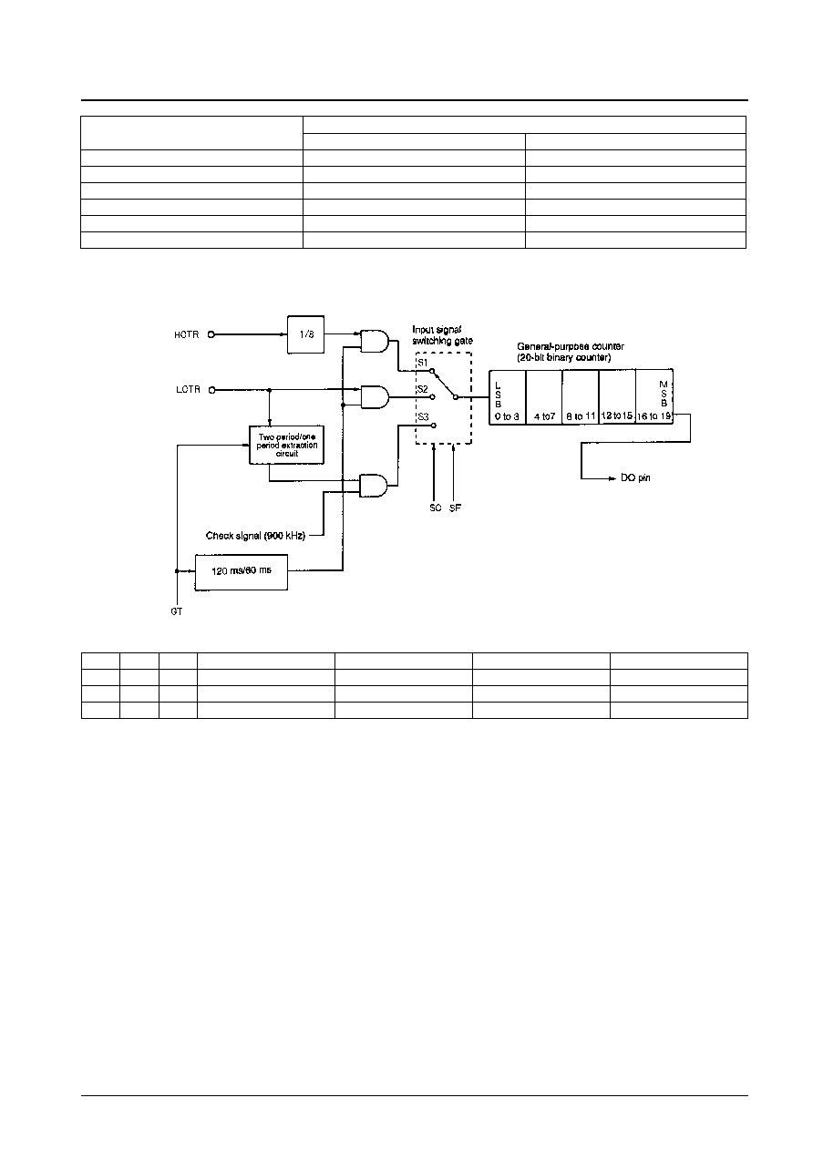
Structure of the General-Purpose Counter
The LC7218 general-purpose counter is a 20-bit binary counter.
The value of the counter can be read out, msb first, from the DO pin.
When the general-purpose counter is used for frequency measurement, GT selects the measurement period to be one of
two periods, 60 or 120 ms. The frequency of the signal input to the HCTR or LCTR pin can be measured by determining
the number of pulses input to the general-purpose counter during the measurement period.
When the general-purpose counter is used for period measurement, the period of the signal input to the LCTR pin can be
measured by determining the number of check signal (900 kHz) cycles input to the general-purpose counter during one
or two periods of the signal input to the LCTR pin.
The general-purpose counter is started by setting CTEN to 1 in the serial data. While the serial data is acquired internally
in the LC7218 at the point the CE signal goes from high to low, the input to the HCTR or LCTR pin must be provided
within 10 ms after CE goes low.
No. 4758-12/16
LC7218, 7218M, 7218JM
Item
Xtal
7.2 MHz
3.6 MHz
Time base clock
8 Hz
4 Hz
System clock
400 kHz
200 kHz
Frequency measurement period
120/60 ms
240/120 ms
Frequency measurement check signal
900 kHz
450 kHz
Reference frequencies
100, 50, 25, ......... 10, 9, 5, 1 kHz
50, 25, 12, 5, .......... 5, 4.5, 2.5, 0.5 kHz
Serial data I/O (CL)
t
1
1.5 µs, t
3
1.5 µs
t
1
3.0 µs, t
3
3.0 µs
SC
SF
Input pin
Measurement item
Measurement frequency range
GT (1/0)
S
1
1
*
HCTR
Frequency measurement
10 to 60 MHz (sine wave)
120 m/60 ms
S
2
0
1
LCTR
Frequency measurement
15 to 500 kHz (sine wave)
120 m/60 ms
S
3
0
0
LCTR
Period measurement
1 Hz to 20 kHz (pulse wave)
Two periods/one period
Next, the value of the general-purpose counter after the measurement completes must be read out while CTEN is still 1.
(The general-purpose counter is reset when CTEN is set to 0.)
Another point that requires care here is that before starting the general-purpose counter, it must be reset by setting
CTEN to 0.
Note that although signals input to the LCTR pin are transmitted directly to the general-purpose counter, signals input to
the HCTR pin are divided by eight internally before being transmitted to the general-purpose counter. Therefore the
value of the general-purpose counter will be 1/8 of the actual frequency input to the HCTR pin.
When counting intermediate frequency signals, always have the controller first check for the presence of the IF-IC SD
(station detect) signal and then only turn on the IF counter buffer output if the SD signal was present. Auto-search
techniques that only use an IF count are subject to stopping at frequencies where there is no station due to leakage output
from the IF counter buffer.
Note that although the DO pin is forced to the high level when the general-purpose counter is started (when CTEN is set
to 1), the DO pin automatically goes low when the measurement completes (after either 60 or 120 ms has elapsed or
when a signal has been applied for one or two periods). Therefore the DO pin can be used to check for measurement
completion.
1. When the general-purpose is not used (when CTEN is 0) the DO pin can be used to check for changes in external
signals.
∑ When mode 3 is specified and data is output through DO, DO will automatically go high after data output has
completed, i.e., when CE goes low.
∑ After that, DO goes low automatically when the IN0 signal changes state.
(That is, DO can be used to check for changes in an external signal input to IN0.)
No. 4758-13/16
LC7218, 7218M, 7218JM
2. When the general-purpose counter is used the DO pin can be used to check for completion of the general-purpose
counter measurement.
∑ When CTEN is set to 1, DO going low due to changes in IN0 is disabled and DO is set high automatically.
∑ DO is automatically set low when the general-purpose counter measurement completes.
(That is, DO can be used to check for measurement completion.)
PLL Unlock Data Read Out Procedure
The internal data UL(n) is set on the rising edge of ¯ERROR
and reset on the rising edge of CE
.
The ¯ERROR data UL(n) from before the previous CE
rising edge can be read out in mode 3 (data output).
In the example above, the data from the period between t
0
and t
1
is read out.
No. 4758-14/16
LC7218, 7218M, 7218JM
UL (n)
3210
¯ERROR < 0.55 µs
0000
0.55 µs
¯ERROR < 1.11 µs
1000
1.11 µs
¯ERROR < 2.22 µs
1001
2.22 µs
¯ERROR < 3.33 µs
1011
3.33 µs
¯ERROR
1111
UL0 : 1.11 µs
UL1 : 2.22 µs
UL2 : 3.33 µs
UL3 : 0.55 µs
Each bit is set to 1 according to ¯ERROR as described above.
¯ERROR: the phase difference (for a 7.2 MHz crystal)
Sample Application System
TV/FM/AM (When IF count is performed)
Note: 1. The coupling capacitors used on the FMIN, AMIN, HCTR, and LCTR pins should be between 50 and 100 pF.
However, a 1000 pF capacitor should be used for LCTR if frequencies under 100 kHz are to be used.
2. Coupling capacitors should be located as close to their pin as possible.
3. When counting intermediate frequency signals, always have the controller first check for the presence of the
IF-IC SD signal and then only turn on the IF counter buffer output if the SD signal was present.
1. TV, 50 kHz steps
When the UHF RF = 637.75 MHz (IF = +10.7 MHz)
TV VCO = 648.45 MHz
PLL fref = 3.125 kHz
DV = 1, SP = * (FMIN selected)
Programmable divider divisor
Set N = 12969 (decimal).
2. FM, 100 kHz steps
When the FM RF = 90 MHz (IF = +10.7 MHz)
FM VCO = 100.7 MHz
PLL fref = 50 kHz
DV = 1, SP = * (FMIN selected)
Programmable divider divisor
Set N = 1007 (decimal).
3. AM, 10 kHz steps
When the AM RF = 1000 kHz (IF = +450 kHz)
AM VCO = 1450 kHz
PLL fref = 10 kHz
DV = 0, SP = 0 (AMIN, low speed measurement selected)
Programmable divider divisor
Set N = 145 (decimal).
*: Do not care
No. 4758-15/16
LC7218, 7218M, 7218JM

No. 4758-16/16
LC7218, 7218M, 7218JM
This catalog provide information as of June, 1996. Specifications and information herein are subject to change
without notice.
s
No products described or contained herein are intended for use in surgical implants, life-support systems, aerospace
equipment, nuclear power control systems, vehicles, disaster/crime-prevention equipment and the like, the failure of
which may directly or indirectly cause injury, death or property loss.
s
Anyone purchasing any products described or contained herein for an above-mentioned use shall:
Accept full responsibility and indemnify and defend SANYO ELECTRIC CO., LTD., its affiliates, subsidiaries and
distributors and all their officers and employees, jointly and severally, against any and all claims and litigation and all
damages, cost and expenses associated with such use:
Not impose any responsibility for any fault or negligence which may be cited in any such claim or litigation on
SANYO ELECTRIC CO., LTD., its affiliates, subsidiaries and distributors or any of their officers and employees
jointly or severally.
s
Information (including circuit diagrams and circuit parameters) herein is for example only; it is not guaranteed for
volume production. SANYO believes information herein is accurate and reliable, but no guarantees are made or implied
regarding its use or any infringements of intellectual property rights or other rights of third parties.