CMOS LSI
Ordering number : EN5378
93096HA (OT) No. 5378-1/13
SANYO Electric Co.,Ltd. Semiconductor Bussiness Headquarters
TOKYO OFFICE Tokyo Bldg., 1-10, 1 Chome, Ueno, Taito-ku, TOKYO, 110 JAPAN
Single-Chip Microcontroller with PLL
and LCD Driver
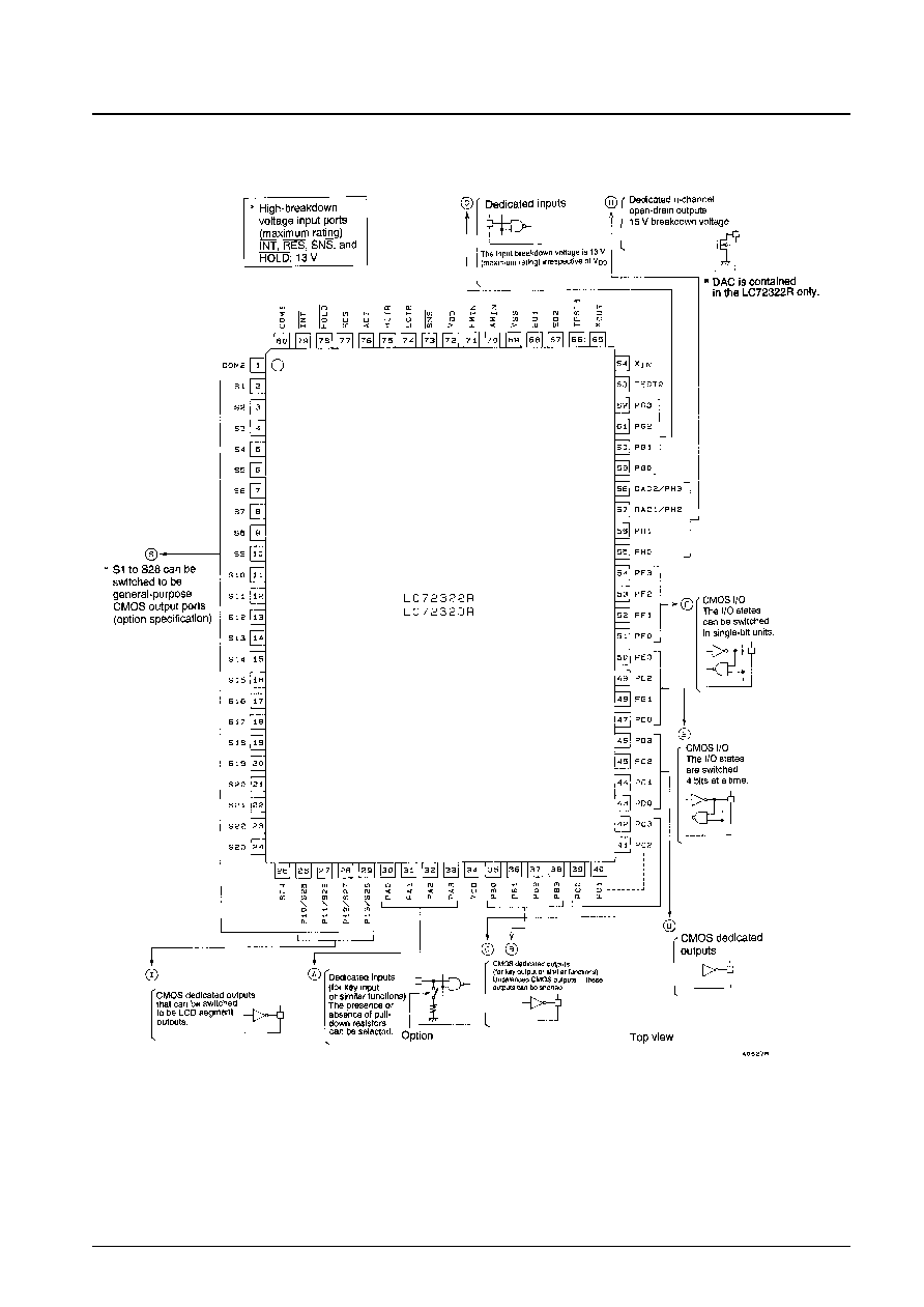
LC72322R, 72323R
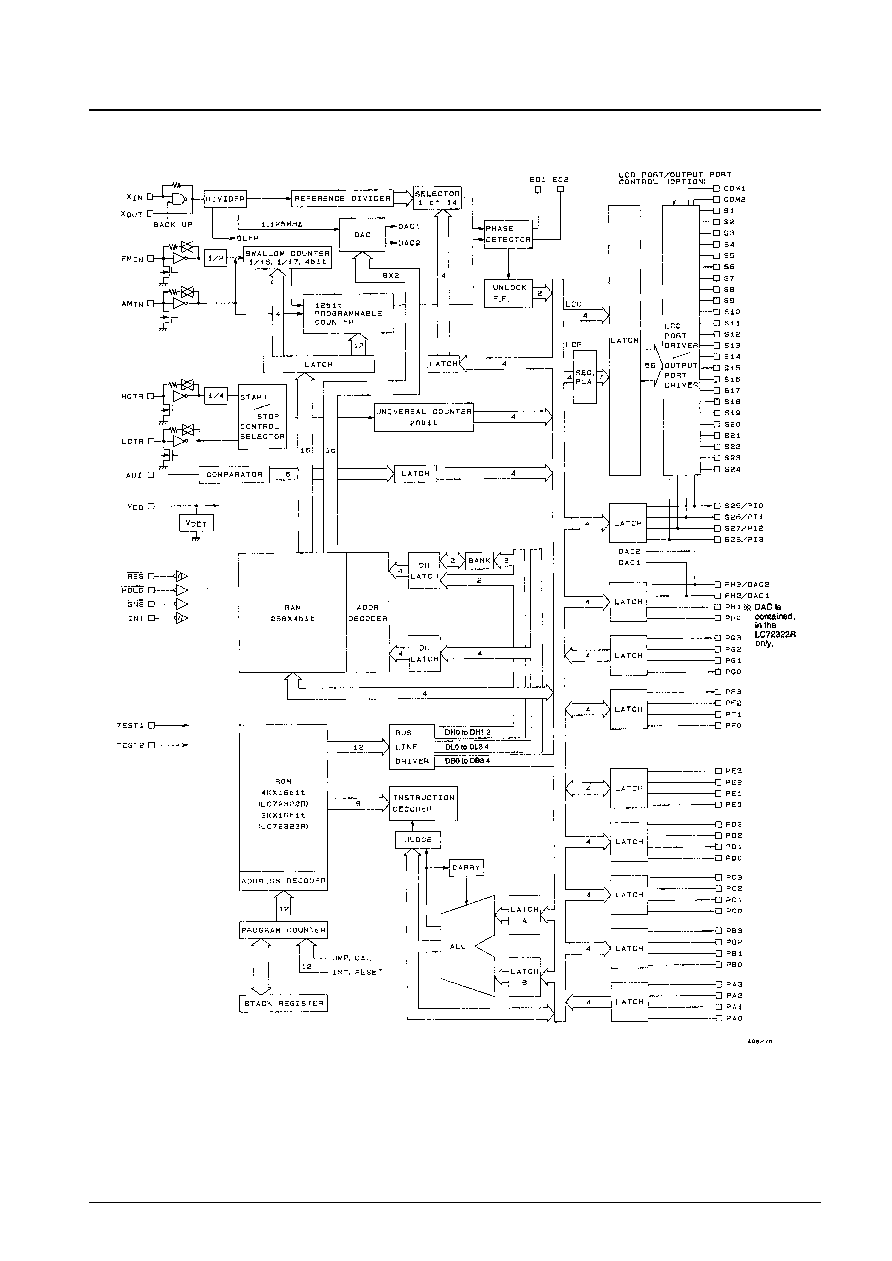
Overview
The LC72322R and LC72323R are single-chip
microcontrollers for use in electronic tuning applications.
These ICs include on chip both LCD drivers and a PLL
circuit that can operate at up to 150 MHz. The LC72322R
and LC72323R feature that these ICs are reversed pin-
assignment versions of LC72322 and LC72323
respectively and have the equal functions and
specifications to theirs respectively.
Functions
∑ Stack: Eight levels
∑ Fast programmable divider
∑ General-purpose counters: HCTR for frequency
measurement and LCTR for frequency or period
measurement
∑ LCD driver for displays with up to 56 segments
(1/2 duty, 1/2 bias)
∑ Program memory (ROM): 4095 (8 KB) 16-bit digits:
LC72322R
3071 (6 KB) 16-bit digits:
LC72323R
∑ Data memory (RAM): 256 4-bit digits
∑ All instructions are single-word instructions
∑ Cycle time:
2.67 µs, 13.33 µs, or 40.00 µs (option)
∑ Unlock FF:
0.55 µs detection, 1.1 µs detection
∑ Timer FF:
1 ms, 5ms, 25ms, 125ms
∑ Input ports*: One dedicated key input port and one
high-breakdown voltage port
∑ Output ports*: Two dedicated key output ports, one
high-breakdown voltage open-drain port
Two CMOS output ports (of which one
can be switched to be used as LCD driver
outputs)
Seven CMOS output ports (mask option
switchable to use as LCD ports)
∑ I/O ports*:
One switchable between input and output
in four-bit units and one switchable
between input and output in bit units
Note: * Each port consists of four bits.
∑ Program runaway can be detected and a special address
set (Programmable watchdog timer).
∑ Voltage detection type reset circuit
∑ One 6-bit A/D converter
∑ Two 8-bit D/A converters (PWM): LC72322R only
∑ One external interrupt
∑ Hold mode for RAM backup
∑ Sense FF for hot/cold startup determination
∑ PLL: 4.5 to 5.5 V
∑ CPU: 3.5 to 5.5 V
∑ RAM: 1.3 to 5.5 V
∑ LC72P321R as OTP used
∑ Package: QIP80DR
Package Dimensions
unit: mm
3223-QFP80DR
This LSI can easily use CCB that is SANYO's original bus format.
∑ CCB is a trademark of SANYO ELECTRIC CO., LTD.
∑ CCB is SANYO's original bus format and all the bus
addresses are controlled by SANYO.
SANYO: QIP80DR
[LC72322R, LC72323R]
Specifications
Absolute Maximum Ratings
at Ta = 25∞C, V
SS
= 0 V
Allowable Operating Ranges
at Ta = ≠40 to +85∞C, V
DD
= 3.5 to 5.5 V
No. 5378-4/13
LC72322R, 72323R
Parameter
Symbol
Conditions
Ratings
Unit
Maximum supply voltage
V
DD
max
≠0.3 to +6.5
V
Input voltage
V
IN
1
HOLD, INT, RES, ADI, SNS, and the G port
≠0.3 to +13
V
V
IN
2
Inputs other than V
IN
1
≠0.3 to V
DD
+ 0.3
V
Output voltage
V
OUT
1
H port
≠0.3 to +15
V
V
OUT
2
Outputs other than V
OUT
1
≠0.3 to V
DD
+ 0.3
V
I
OUT
1
All D and H port pins
0 to 5
mA
Output current
I
OUT
2
All E and F port pins
0 to 3
mA
I
OUT
3
All B and C port pins
0 to 1
mA
I
OUT
4
S1 to S28 and all I port pins
0 to 1
mA
Allowable power dissipation
Pd max
Ta = ≠40 to +85∞C
300
mW
Operating temperature
Topr
≠40 to +85
∞C
Storage temperature
Tstg
≠45 to +125
∞C
Parameter
Symbol
Conditions
Ratings
Unit
min
typ
max
V
DD
1
CPU and PLL operating
4.5
5.5
V
Supply voltage
V
DD
2
CPU operating
3.5
5.5
V
V
DD
3
Memory retention voltage
1.3
5.5
V
V
IH
1
G port
0.7 V
DD
8.0
V
V
IH
2
RES, INT, HOLD
0.8 V
DD
8.0
V
Input high level voltage
V
IH
3
SNS
2.5
8.0
V
V
IH
4
A port
0.6 V
DD
V
DD
V
V
IH
5
PE0, PE2 and F ports
0.7 V
DD
V
DD
V
V
IH
6
LCTR (period measurement),
0.8 V
DD
V
DD
V
V
DD
1, PE1 and PE3
V
IL
1
G port
0
0.3 V
DD
V
V
IL
2
RES, INT, PE1, PE3
0
0.2 V
DD
V
V
IL
3
SNS
0
1.3
V
Input low level voltage
V
IL
4
A port
0
0.2 V
DD
V
V
IL
5
PE0, PE2 and F ports
0
0.3 V
DD
V
V
IL
6
LCTR (period measurement), V
DD
1
0
0.2 V
DD
V
V
IL
7
HOLD
0
0.4 V
DD
V
f
IN
1
XIN
4.0
4.5
5.0
MHz
f
IN
2
FMIN, V
IN
2, V
DD
1
10
130
MHz
f
IN
3
FMIN, V
IN
3, V
DD
1
10
150
MHz
Input frequency
f
IN
4
AMIN (L), V
IN
4, V
DD
1
0.5
10
MHz
f
IN
5
AMIN (H), V
IN
5, V
DD
1
2.0
40
MHz
f
IN
6
HCTR, V
IN
6, V
DD
1
0.4
12
MHz
f
IN
7
LCTR (frequency), V
IN
7, V
DD
1
100
500
kHz
f
IN
8
LCTR (period), V
IH
6, V
IL
6, V
DD
1
1
20
◊
10
3
Hz
V
IN
1
XIN
0.50
1.5
Vrms
V
IN
2
FMIN
0.10
1.5
Vrms
Input amplitude
V
IN
3
FMIN
0.15
1.5
Vrms
V
IN
4, 5
AMIN
0.10
1.5
Vrms
V
IN
6, 7
LCTR, HCTR
0.10
1.5
Vrms
Input voltage range
V
IN
8
ADI
0
V
DD
V
Electrical Characteristics
for the Allowable Operating Ranges
No. 5378-5/13
LC72322R, 72323R
Parameter
Symbol
Conditions
Ratings
Unit
min
typ
max
Hysteresis
V
H
LCTR (period), RES, INT, PE1, PE3
0.1 V
DD
V
Rejected pulse width
P
REJ
SNS
50
µs
Power-down detection voltage
V
DET
2.7
3.0
3.3
V
I
IH
1
INT, HOLD, RES, ADI, SNS,
3.0
µA
and G port: V
I
= 5.5 V
I
IH
2
A, E, and F ports: E and F ports with
3.0
µA
Input high level current
outputs off, A port with no R
PD
, VI = V
DD
I
IH
3
XIN: V
I
= V
DD
= 5.0 V
2.0
5.0
15
µA
I
IH
4
FMIN, AMIN, HCTR, LCTR:
4.0
10
30
µA
V
I
= V
DD
= 5.0 V
I
IH
5
A port: With an R
PD
, V
I
= V
DD
= 5.0 V
50
µA
I
IL
1
INT, HOLD, RES, ADI, SNS,
3.0
µA
and the G port: V
I
= V
SS
Input low level current
I
IL
2
A, E, and F ports: E and F ports with
3.0
µA
outputs off, A port with no R
PD
, V
I
= V
SS
I
IL
3
XIN: V
IN
= V
SS
2.0
5.0
15
µA
I
IL
4
FMIN, AMIN, HCTR, LCTR: V
I
= V
SS
4.0
10
30
µA
Input floating voltage
V
IF
A port: With an R
PD
0.05 V
DD
V
Pull-down resistance
R
PD
A port: With an R
PD
, V
DD
= 5.0 V
75
100
200
k
I
OFFH
1
EO1, EO2: V
O
= V
DD
0.01
10
nA
Output high level off leakage current
I
OFFH
2
B, C, D, E, F, and I ports: V
O
= V
DD
3.0
µA
I
OFFH
3
H port: V
O
= V
DD
5.0
µA
Output low level off leakage current
I
OFFL
1
EO1, EO2: V
O
= V
SS
0.01
10
nA
I
OFFL
2
B, C, D, E, F, and I ports: V
O
= V
SS
3.0
µA
V
OH
1
B and C ports: I
O
= 1 mA
V
DD
≠ 2.0
V
DD
≠ 1.0
V
DD
≠ 0.5
V
V
OH
2
E and F ports: I
O
= 1 mA
V
DD
≠ 1.0
V
V
OH
3
EO1, EO2: I
O
= 500 µA
V
DD
≠ 1.0
V
Output high level voltage
V
OH
4
XOUT: I
O
= 200 µA
V
DD
≠ 1.0
V
V
OH
5
S1 to S28 and the I port: I
O
= ≠0.1 mA
V
DD
≠ 1.0
V
V
OH
6
D port: I
O
= 5 mA
V
DD
≠ 1.0
V
V
OH
7
COM1, COM2: I
O
= 25 µA
V
DD
≠ 0.75
V
DD
≠ 0.5
V
DD
≠ 0.3
V
V
OL
1
B and C ports: I
O
= 50 µA
0.5
1.0
2.0
V
V
OL
2
E and F ports: I
O
= 1 mA
1.0
V
V
OL
3
EO1, EO2: I
O
= 500 µA
1.0
V
Output low level voltage
V
OL
4
XOUT: I
O
= 200 µA
1.0
V
V
OL
5
S1 to S28 and the I port: I
O
= 0.1 mA
1.0
V
V
OL
6
D port: I
O
= 5 mA
1.0
V
V
OL
7
COM1, COM2: I
O
= 25 µA
0.3
0.5
0.75
V
V
OL
8
H port: I
O
= 5 mA, V
DD
1
(150
) 0.75
(400
) 2.0
V
Output middle level voltage
V
M
1
COM1, COM2: V
DD
= 5.0 V, I
O
= 25 µA
2.0
2.5
3.0
V
A/D conversion error
ADI: V
DD
1
≠1/2
+1/2
LSB
I
DD
1
V
DD
1, f
IN
2 = 130 MHz
15
20
mA
I
DD
2
V
DD
2, PLL stopped, CT = 2.67 µs
1.5
mA
(HOLD mode, Figure 1)
I
DD
3
V
DD
2, PLL stopped, CT = 13.33 µs
1.0
mA
(HOLD mode, Figure 1)
Current drain
I
DD
4
V
DD
2, PLL stopped, CT = 40.00 µs
0.7
mA
(HOLD mode, Figure 1)
V
DD
= 5.5 V, oscillator stopped, Ta = 25∞C
5
µA
I
DD
5
(BACK UP mode, Figure 2)
V
DD
= 2.5 V, oscillator stopped, Ta = 25∞C
1
µA
(BACK UP mode, Figure 2)