 | –≠–ª–µ–∫—Ç—Ä–æ–Ω–Ω—ã–π –∫–æ–º–ø–æ–Ω–µ–Ω—Ç: LC72346W | –°–∫–∞—á–∞—Ç—å:  PDF PDF  ZIP ZIP |
Ordering number : ENN
*
6651
N1501TN (OT) No. 6651-1/12
Overview
The LC72346W and LC72347W are ultralow-voltage
electronic tuning microcontrollers that include a PLL that
operates up to 250 MHz and a 1/4 duty 1/2 bias LCD
driver on chip. This IC includes an on-chip DC-DC
converter that can easily create the power supply voltages
needed for electronic tuning and contribute to reducing
end product costs. This IC is optimal for portable audio
equipment that must operate from a single battery.
Function
∑ Program memory (ROM):
-- 4096
◊
16 bits (8K bytes) : LC72346
-- 6144
◊
16 bits (12K bytes): LC72347
∑ Data memory (RAM):
-- 256
◊
4 bits: LC72346
-- 512
◊
4 bits: LC72347
∑ Cycle time:
40 µs (all 1-word instructions) at 75kHz crystal oscillation
∑ Stack: 8 levels
∑ LCD driver: 48 to 80 segments (1/4 duty, 1/2 bias drive)
∑ Interrupts: Two external interrupts
Timer interrupts (1, 5, 10, and 50 ms)
∑ A/D converter:
Four input channels (6-bit successive approximation
conversion)
∑ Input ports: 7 ports (of which three can be switched for
use as A/D converter inputs)
∑ Output ports: 6 ports (of which 1 can be switched for use
as the beep tone output and 2 are open-drain ports)
∑ I/O ports: 20 ports (of which 8 can be switched for use
as LCD ports and as mask options, of which 3 can be
switched for use as serial I/O ports)
∑ Serial I/O: One system (LC72347)
∑ PLL: Reference frequencies:
1, 3, 3.125, 5, 6.25, 12.5, and 25 kHz
∑ Input frequencies: FM band: 10 to 250 MHz
AM band (high): 2 to 20 MHz
AM band (low): 0.5 to 10 MHz
∑ Input sensitivity:
FM band: 35 mVrms (50 mVrms at 130 MHz or higher
frequency)
AM band (high, low): 35 mVrms
∑ External reset input: During CPU and PLL operations,
instruction execution is started from location 0.
∑ Built-in power-on reset circuit:
The CPU starts execution from location 0 when power is
first applied.
∑ Halt mode: The controller-operating clock is stopped.
Continued on next page.
Package Dimensions
unit: mm
3190-SQFP64
10.0
12.0
1.25
0.5
1.25
1.25
0.5
1.25
0.18
12.0
1
16
17
32
33
48
49
64
10.0
0.5
1.7max
0.5
0.1
0.15
Preliminary
SANYO: SQFP64
[LC72346W, 72347W]
LC72346W, 72347W
SANYO Electric Co.,Ltd. Semiconductor Company
TOKYO OFFICE Tokyo Bldg., 1-10, 1 Chome, Ueno, Taito-ku, TOKYO, 110-8534 JAPAN
Ultralow-Voltage ETR Controller
with On-Chip LCD Driver
CMOS IC
Any and all SANYO products described or contained herein do not have specifications that can handle
applications that require extremely high levels of reliability, such as life-support systems, aircraft's
control systems, or other applications whose failure can be reasonably expected to result in serious
physical and/or material damage. Consult with your SANYO representative nearest you before using
any SANYO products described or contained herein in such applications.
SANYO assumes no responsibility for equipment failures that result from using products at values that
exceed, even momentarily, rated values (such as maximum ratings, operating condition ranges, or other
parameters) listed in products specifications of any and all SANYO products described or contained
herein.
No. 6651-2/12
LC72346W, 72347W
Continued from preceding page.
∑ Backup mode: The crystal oscillator is stopped.
∑ Static power-on function:
Backup state is cleared with the PF port
∑ Beep tone: 1.5 and 3.1 kHz
∑ Built-in DC-DC converter:
For LCD and A/D converter use (3 V)
Can also be used for TU + B creation by using a
secondary coil.
∑ Built-in remaining battery life verification function:
Converts the V
DD
pin level to digital.
∑ Memory retention voltage: 0.5 V or higher
∑ Dedicated memory power supply: The RAM retention
time has been increased by the provision of a dedicated
memory power supply.
∑ Package: SQFP-64 (0.5-mm pitch)
∑ V
DD
power supply: 0.9 to 1.8 V
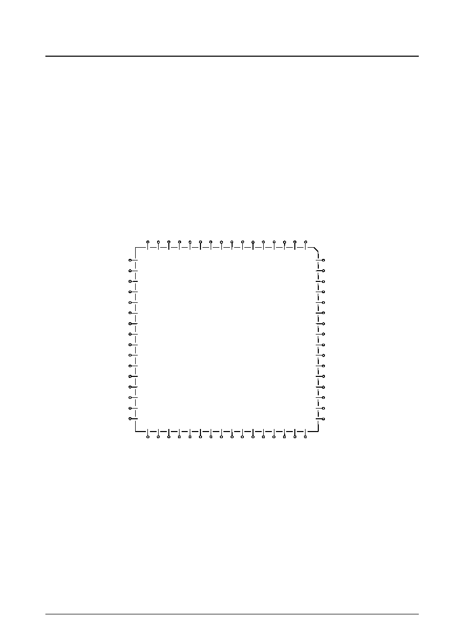
Pin Assignment
61
62
63
S3
S2
S1
COM4
COM3
COM2
S4
INT1/PD1
INT0/PD0
PE1
BEEP/PE0
ADI3/PF2
ADI1/PF1
ADI0/PF0
SI1/P
K3
SO1/PK2
SCK1/PK1
PK0
VSS
VDDRAM
VDC3
VDC1
VADJ
BRES
VDD
FMIN
VSS
AMIN
EO
TEST1
XIN
COM1
64
58
59
60
55
56
57
52
53
54
49
50
51
48
47
46
45
44
43
42
41
40
39
38
37
36
35
34
15
16
33
31 32
29 30
27 28
25 26
23 24
21 22
19 20
17 18
13
14
11
12
9
10
7
8
5
6
3
4
S5
XOUT
1
S6
TEST2
S7
PA3
S8
PA2
S9
PA1
S10
LC72346W
LC72347W
PA0
S11
PB3
S12
PB2
S13/PH0
PB1
S14/PH1
PB0
S15/PH2
PC3
S16/PH3
PC2
S17/PG0
PC1
S18/PG1
PC0
S19/PG2
PD3
PD2
S20/PG3
2
No. 6651-3/12
LC72346W, 72347W
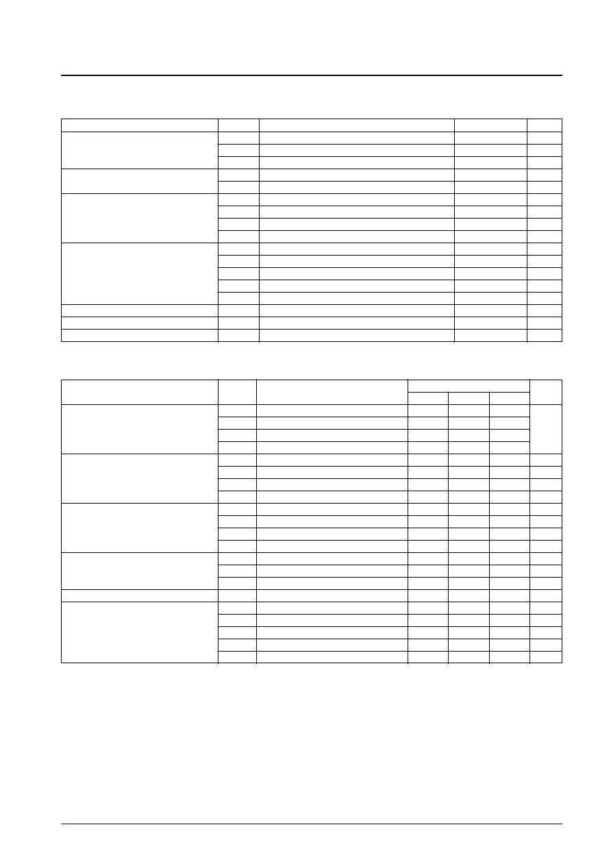
Parameter
Symbol
Conditions
Ratings
Unit
V
DD
1 max
V
DD
≠0.3 to +3.0
V
Maximum supply voltage
V
DD
3 max
V
DD
RAM
≠0.3 to +4.0
V
V
DD
4 max
VDC3
≠0.3 to +4.0
V
Input voltage
V
IN
1
FMIN, AMIN
≠0.3 to V
DD
1 +0.3
V
V
IN
2
PA, PC, PD, PF, PK, PG, PH, BRES
≠0.3 to V
DD
1 +0.3
V
V
OUT
1
PE
≠0.3 to +7
V
Output voltage
V
OUT
2
PB, PC, PD, PG, PH
≠0.3 to V
DD
1 +0.3
V
V
OUT
3
VDC1, EO
≠0.3 to V
DD
4 +0.3
V
V
OUT
4
COM1 to COM4, S1 to S20
≠0.3 to V
DD
4 +0.3
V
I
OUT
1
PC, PD, PG, PH, EO
0 to 3
mA
I
OUT
2
PB
0 to 1
mA
Output current
I
OUT
3
PE
0 to 2
mA
I
OUT
4
S1 to S20
300
µA
I
OUT
5
COM1 to COM4
3
mA
Allowable power dissipation
Pdmax
Ta = ≠10 to +60∞C
100
mW
Operating temperature
Topr
≠10 to +60
∞C
Storage temperature
Tstg
≠45 to +125
∞C
Specifications
Absolute Maximum Ratings
at Ta = 25∞C, V
SS
= 0 V
Parameter
Symbol
Conditions
Ratings
Unit
min
typ
max
V
DD
1
Voltage applied to the V
DD
pin
0.9
1.3
1.8
Supply voltage
V
DD
3
Voltage applied to the V
DD
RAM pin
2.7
3.0
3.3
V
V
DD
4
Voltage applied to the VDC3 pin
2.7
3.0
3.3
V
DD
5
Memory retention voltage
0.5
V
IH
1
Ports PC, PD, PG, PH, and PK
0.7 V
DD
1
V
DD
1
V
Input high-level voltage
V
IH
2
Port PA
0.8 V
DD
1
V
DD
1
V
V
IH
3
Port PF
0.8 V
DD
1
V
DD
1
V
V
IH
4
Port BRES
0.6 V
DD
1
V
DD
1
V
V
IL
1
Ports PC, PD, PG, PH, and PK
0
0.3 V
DD
1
V
Input low-level voltage
V
IL
2
Port PA
0
0.2 V
DD
1
V
V
IL
3
Port PF
0
0.2 V
DD
1
V
V
IL
4
Port BRES
0
0.2 V
DD
1
V
V
IN
1
XIN
0.5
0.6
Vrms
Input amplitude
V
IN
2
FMIN, AMIN: V
DD
1 = 0.9 to 1.8 V
0.035
0.35
Vrms
V
IN
3
FMIN: V
DD
1 = 0.9 to 1.8 V
0.05
0.35
Vrms
Input voltage range
V
IN
4
ADI0, ADI1, ADI3, V
DD
1
0
V
DD
4
V
F
IN
1
XIN: CI
35 k
70
75
80
kHz
F
IN
2
FMIN: V
IN
2, V
DD
1 = 0.9 to 1.8 V
10
130
MHz
Input frequency
F
IN
3
FMIN: V
IN
3, V
DD
1 = 0.9 to 1.8 V
130
250
MHz
F
IN
4
AMIN(L): V
IN
2, V
DD
1 = 0.9 to 1.8 V
0.5
10
MHz
F
IN
5
AMIN(H): V
IN
2, V
DD
1 = 0.9 to 1.8 V
2.0
20
MHz
Allowable Operating Ranges
at Ta = ≠10 to +60∞C, V
DD
= 0.9 to 1.8 V
No. 6651-4/12
LC72346W, 72347W
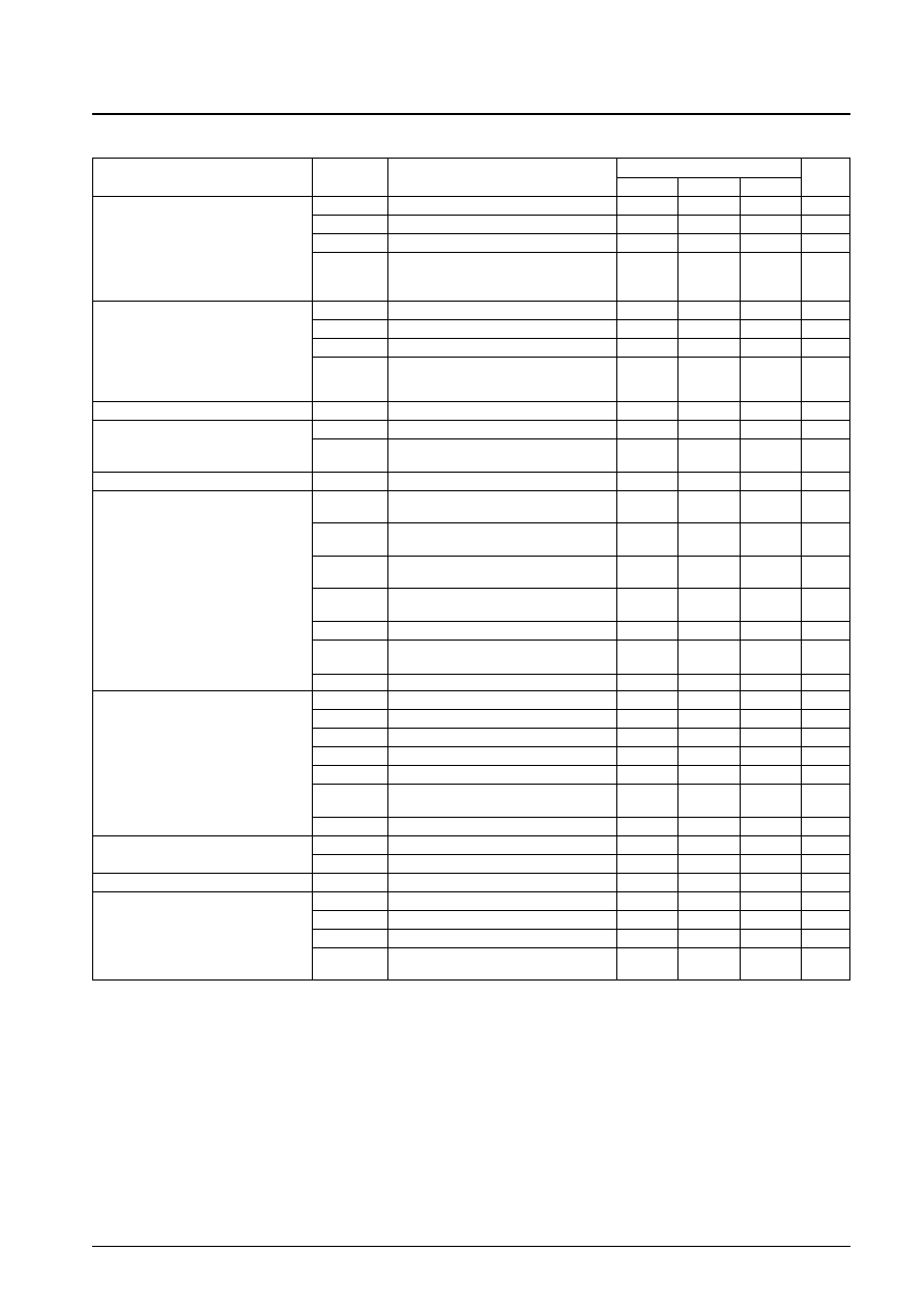
Parameter
Symbol
Conditions
Ratings
Unit
min
typ
max
I
IH
1
XIN: V
DD
1 = 1.3 V
3
µA
I
IH
2
FMIN, AMIN: V
DD
1 = 1.3 V
3
8
20
µA
Input high-level current
I
IH
3
Port PF: V
DD
1 = 1.3 V
4
µA
PA (without pull-down resistors), the PC,
I
IH
4
PD, PG, and PH ports, and BRES,
3
µA
PK: V
DD
1 = 1.3 V
I
IL
1
XIN: V
DD
1 = V
SS
≠3
µA
I
IL
2
FMIN, AMIN: V
DD
1 = V
SS
≠3
≠8
≠20
µA
Input low-level current
I
IL
3
Port PF: V
DD
1 = V
SS
≠4
µA
I
IL
4
PA (without pull-down resistors), the PC,
PD, PG, and PH ports, and BRES,
≠3
µA
PK: V
DD
1 = V
SS
Input floating voltage
V
IF
PA (with pull-down resistors)
0.05 V
DD
1
V
R
PD
1
PA/PF (with pull-down resistors), V
DD
1 = 1.3 V
75
100
200
k
Pull-down resistor values
R
PD
2
TEST1, TEST2 (with pull-down resistors),
10
k
V
DD
1 = 1.3 V
Hysteresis
V
H
BRES
0.1 V
DD
1
0.2 V
DD
1
V
V
OH
1
PB: I
O
= 1 mA
V
DD
1 ≠
V
0.3 V
DD
V
OH
2
PC, PD, PG, PH and PK: I
O
= 1 mA
V
DD
1 ≠
V
0.3 V
DD
1
V
OH
3
EO: I
O
= 500 µA
V
DD
4 ≠
V
0.3 V
DD
4
Output high-level voltage
V
OH
4
XOUT: I
O
= 1 µA
V
DD
1 ≠
V
0.3 V
DD
1
V
OH
5
S1 to S20: I
O
= 20 µA
V
DD
4 ≠1
V
V
OH
6
COM1, COM2, COM3, COM4:
V
DD
4 ≠1
V
I
O
= 100 µA
V
OH
7
VDC1: I
O
= 1 mA
V
DD
4 ≠1
V
V
OL
1
PB: I
O
= ≠50 µA
0.3 V
DD
1
V
V
OL
2
PC, PD, PG, PH and PK: I
O
= ≠1 mA
0.3 V
DD
1
V
V
OL
3
EO: I
O
= ≠500 µA
0.3 V
DD
4
V
Output low-level voltage
V
OL
4
XOUT: I
O
= ≠1 µA
0.3 V
DD
1
V
V
OL
5
S1 to S20: I
O
= ≠20 µA
V
DD
4 ≠2
V
V
OL
6
COM1, COM2, COM3, COM4:
V
DD
4 ≠2
V
I
O
= ≠100 µA
V
OL
7
PE: I
O
= 2 mA
0.6 V
DD
1
V
Output off leakage current
I
OFF
1
Ports PB, PC, PD, PG, PK, and EO
≠3
+3
µA
I
OFF
2
Port PE
≠100
+100
nA
A/D converter error
ADI0, ADI1, ADI3 V
DD
1
≠1/2
+1/2
LSB
I
DD
1
V
DD
1 = 1.3 V: F
IN
2 130 MHz, Ta = 25∞C
10
30
mA
I
DD
2
V
DD
1 = 1.3 V: In PLL stop mode, Ta = 25∞C
0.15
mA
Current drain
I
DD
3
V
DD
1 = 1.3 V: In HALT mode, Ta = 25∞C
*
1
0.1
mA
I
DD
4
V
DD
1 = 1.8 V, with the oscillator stopped,
1
µA
Ta = 25∞C
*
2
Electrical Characteristics
under allowable operating conditions
Note
*
: The halt mode current drain is due to 20 instructions being executed every 125 ms.
No. 6651-5/12
LC72346W, 72347W
A
7 pF
FMIN
XIN
AMIN
TEST1, 2
XOUT
VDD
VDC3
RES
VSS
PA, PF, PK
7 pF
75 kHz
VADJ
3 V
A
7 pF
FMIN
XIN
AMIN
TEST1, 2
XOUT
VDD
VDC3
RES
VSS
7 pF
75 kHz
VADJ
3 V
VADJ
VDC3
VDDRAM
VDC1
VSS
VDD
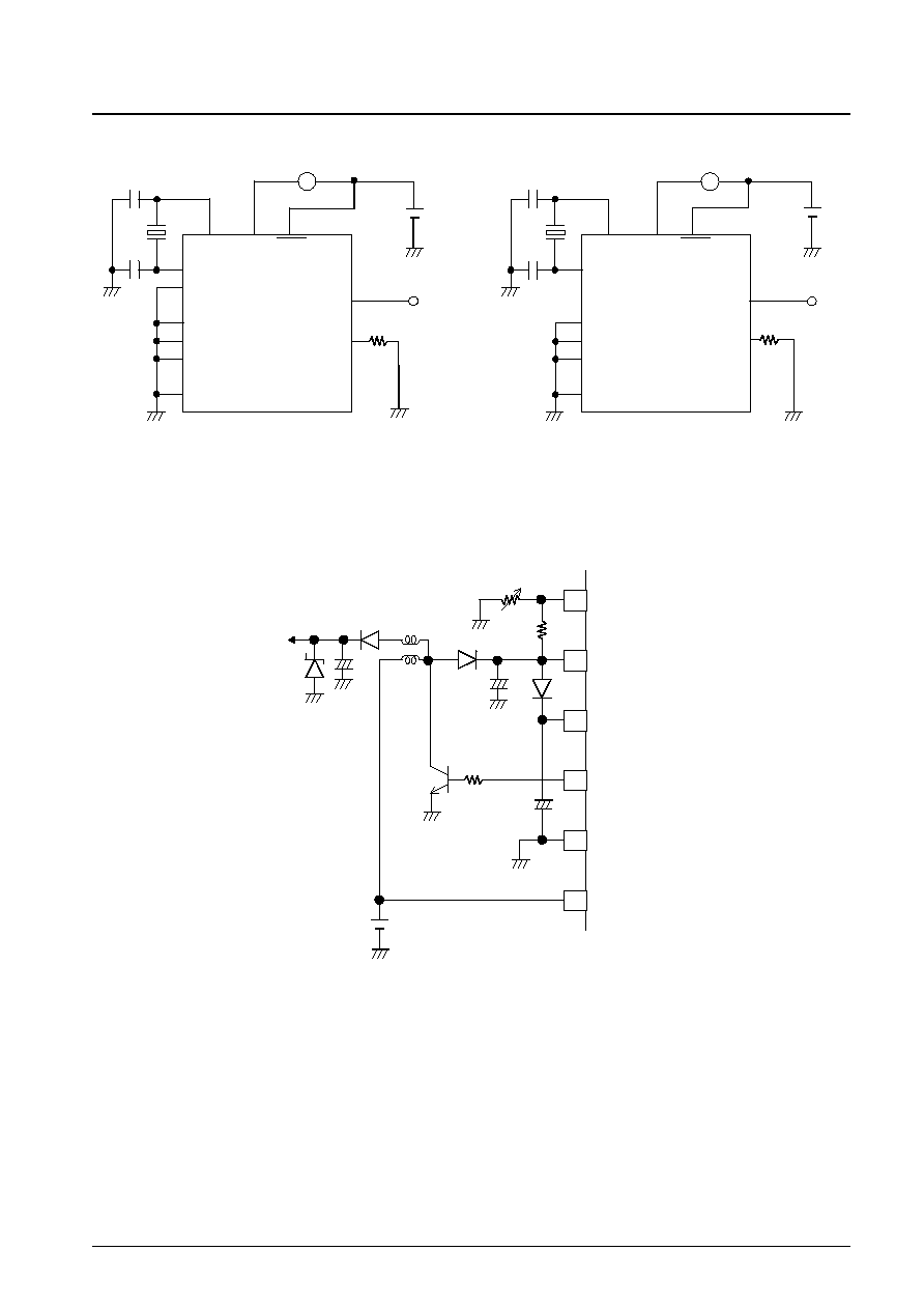
*1. Halt and PLL STOP mode current test circuit
*2. Backup mode current test circuit
With all ports other than those specified above left open.
With output mode selected for PC and PD.
With segments S13 to S20 selected.
With all ports other than those specified above left open.
With output mode selected for PC and PD.
With segments S13 to S20 selected.
DC-DC Converter Application