 | –≠–ª–µ–∫—Ç—Ä–æ–Ω–Ω—ã–π –∫–æ–º–ø–æ–Ω–µ–Ω—Ç: LC723483W | –°–∫–∞—á–∞—Ç—å:  PDF PDF  ZIP ZIP |
Ordering number : ENN7253
N2002RM (OT) No. 7253-1/15
Overview
The LC723481W, 723482W, and 723483W are low-
voltage electronic tuning radio microcontrollers that
include a PLL that operates up to 250 MHz and a 1/4 duty
1/2 bias LCD driver on chip. These ICs include an on-chip
DC-DC converter, making it is easy to create the supply
voltages required for tuning and allowing cost reductions
in end products.
These ICs are optimal for use in low-voltage portable
audio equipment that includes a radio receiver.
Function
∑ Program memory (ROM):
-- 2048
◊
16 bits (4K bytes)
LC723481W
-- 3072
◊
16 bits (6K bytes)
LC723482W
-- 4096
◊
16 bits (8K bytes)
LC723483W
∑ Data memory (RAM):
-- 128
◊
4 bits
LC723481W
-- 192
◊
4 bits
LC723482W
-- 256
◊
4 bits
LC723483W
∑ Cycle time: 40 µs (all 1-word instructions) at 75kHz
crystal oscillation
∑ Stack: 4 levels (8 levels)
LC723481W(LC723482W/3W)
∑ LCD driver: 48 to 80 segments (1/4 duty, 1/2 bias drive)
∑ Interrupts: One external interrupt
Timer interrupts (1, 5, 10, and 50 ms)
∑ A/D converter: Three input channels
(5-bit successive approximation
conversion)
∑ Input ports: 7 ports (of which 3 can be switched for use
as A/D converter inputs)
∑ Output ports: 6 ports (of which 1 can be switched for use
as the beep tone output and 2 are open-
drain ports)
Continued on next page.
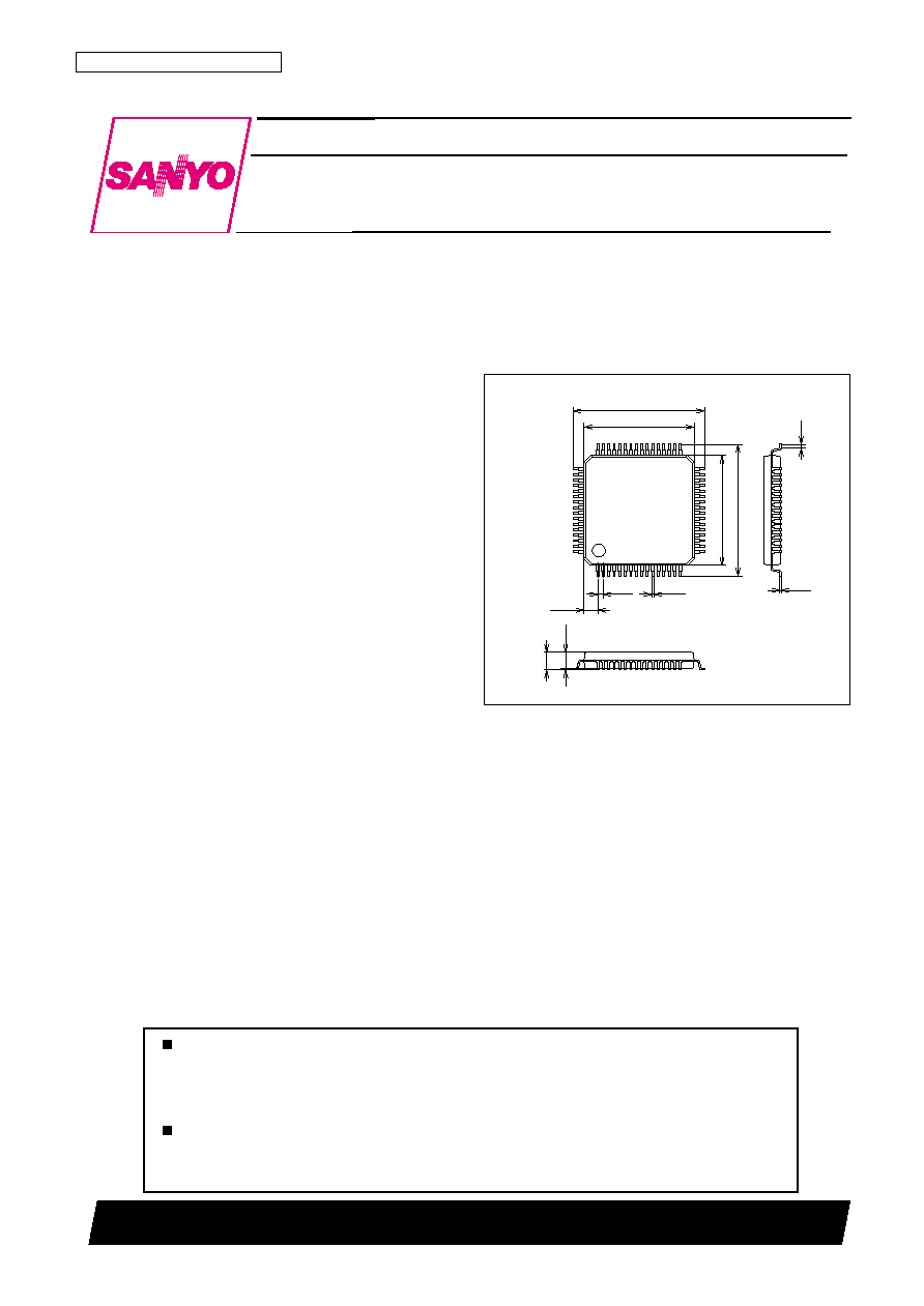
Package Dimensions
unit: mm
3190A-SQFP64
10.0
10.0
12.0
12.0
0.15
0.5
(1.5)
0.1
1.7max
0.18
(0.5)
(1.25)
1
16
17
32
33
48
49
64
SANYO: SQFP64
[LC723481W/2W/3W]
LC723481W,723482W,723483W
SANYO Electric Co.,Ltd. Semiconductor Company
TOKYO OFFICE Tokyo Bldg., 1-10, 1 Chome, Ueno, Taito-ku, TOKYO, 110-8534 JAPAN
Low-Voltage ETR-Controller
CMOS IC
Any and all SANYO products described or contained herein do not have specifications that can handle
applications that require extremely high levels of reliability, such as life-support systems, aircraft's
control systems, or other applications whose failure can be reasonably expected to result in serious
physical and/or material damage. Consult with your SANYO representative nearest you before using
any SANYO products described or contained herein in such applications.
SANYO assumes no responsibility for equipment failures that result from using products at values that
exceed, even momentarily, rated values (such as maximum ratings, operating condition ranges, or other
parameters) listed in products specifications of any and all SANYO products described or contained
herein.
No. 7253-2/15
LC723481W/2W/3W
Continued from preceding page.
I/O ports: 16 pins (Of these 8 can be switched over to
function as LCD ports as a mask options.)
∑ PLL: Dead band control is supported. (Four types)
Reference frequencies: 1, 3, 3.125, 5, 6.25, 12.5,
and 25 kHz
∑ Input frequencies: FM band: 10 to 250 MHz
AM band: 0.5 to 40 MHz
∑ Input sensitivity:
FM band: 35 mVrms (50 mVrms at 130 MHz or higher
frequency)
AM band: 35 mVrms
∑ IF counting: Using the HCTR input pin for 0.4 to
12 MHz signals
∑ External reset input: During CPU and PLL operations,
instruction execution is started from
location 0.
∑ Built-in power-on reset circuit:
The CPU starts execution from location 0 when power is
first applied.
∑ Halt mode: The controller-operating clock is stopped.
∑ Backup mode: The crystal oscillator is stopped.
∑ Static power-on function: Backup state is cleared with
the PF port
∑ Beep tone: 1.5625 and 3.125 kHz
∑ Built-in low-pass filter amplifier: This circuit obviates
the need for an external amplifier for the PLL circuit and
contributes to reduced end product costs.
∑ Built-in DC/DC converter:
Cost reduced in tuner-use power supply circuit
∑ Memory retention voltage: 0.9 V at least
∑ V
DD
voltage
-- PLL: 1.8 to 3.6 V
-- CPU: 1.4 to 3.6 V
-- ADC: 1.6 to 3.6 V
∑ Optional function switches:
-- PH0 to PH3/S13 to S16
-- PG0 to PG3/S17 to S20
-- PG0 to PG3 (open-drain output/general-purpose
output)
-- PH0 to PH3 (open-drain output/general-purpose
output)
-- FM DC/DC clock (75 kHz or 1/256 times the local
FM oscillator frequency)
-- AM DC/DC clock (1/2, 1/4, 1/8, or 1/16 times the
AM local oscillator frequency)
∑ Package: SQFP-64 (0.5-mm pitch)
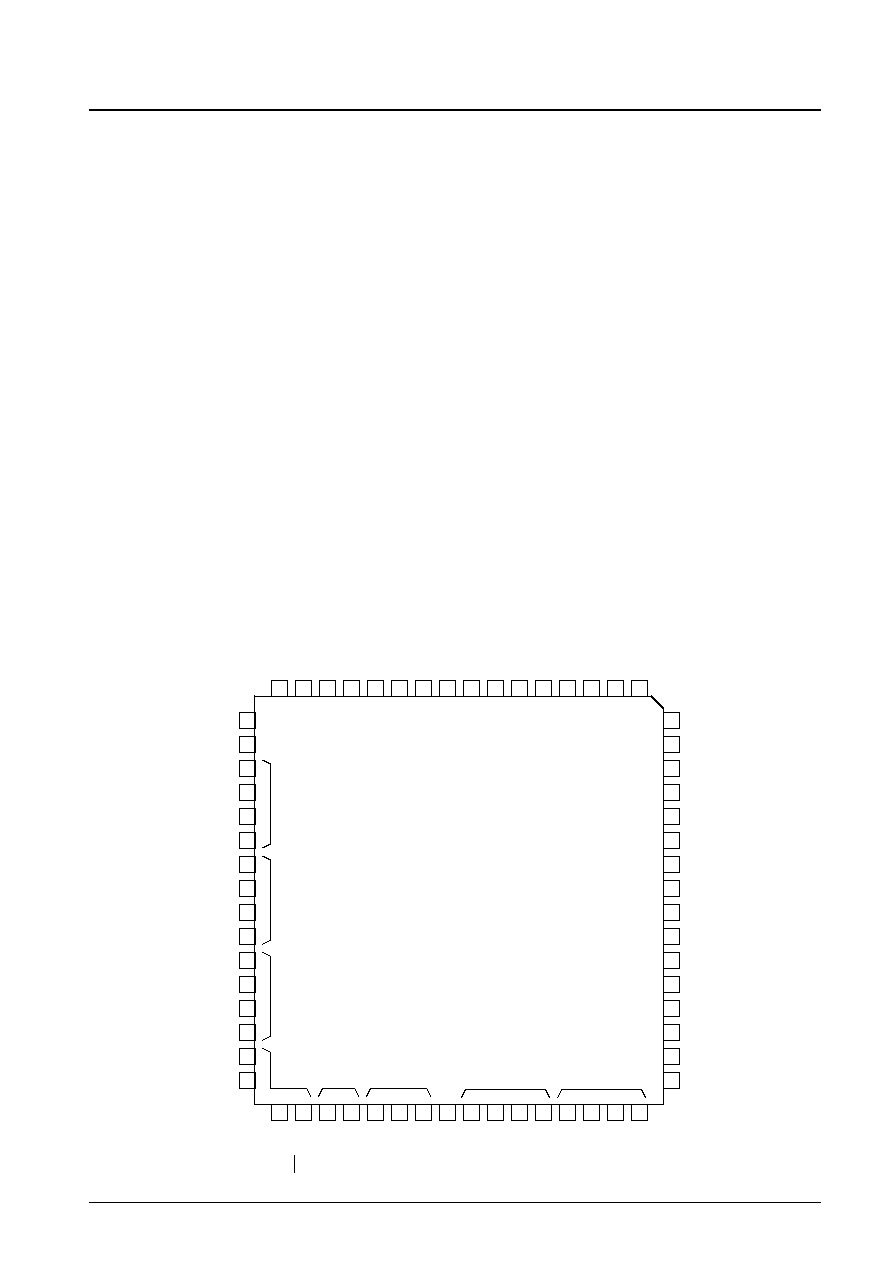
Pin Assignment
XOUT
TEST2
PA3
PB3
PC3
PD3
PD2
S12
S11
S10
S9
S8
S7
S6
S5
S4
S3
S2
S1
COM4
COM3
COM2
COM1
PC2
PC1
PC0
PB2
PB1
PB0
PA2
PA1
PA0
PD2
PE1
BEEP/PE0
ADI3/PF2
ADI1/PF1
ADI0/PF0
S20/PG3
S16/PH3
S15/PH2
S14/PH1
S13/PH0
S19/PG2
S18/PG1
S17/PG0
V
SS
INT/PD0
63
64
61
62
58
59
60
56
57
54
55
52
53
49
50
1
48
2
47
51
46
45
44
43
42
41
40
39
38
37
36
35
34
33
31
32
3
4
5
6
7
8
9
10
11
12
13
14
15
16
28
29
30
26
27
24
25
22
23
17
18
19
20
21
DBR4
TU
DBR3
DBR2
DBR1
BRES
HCTR
V
DD
V
SS
FMIN
AMIN
EO
AIN
XIN
General-purpose
inputs
General-purpose unbalanced outputs
Open drain outputs
General-purpose I/O
Open drain
outputs
General-purpose inputs/
A/D converter inputs
General-purpose I/O,
open drain outputs,
segment outputs
General-purpose I/O,
open drain outputs,
segment outputs
General-
purpose
I/O
TEST1
AOUT
No. 7253-3/15
LC723481W/2W/3W
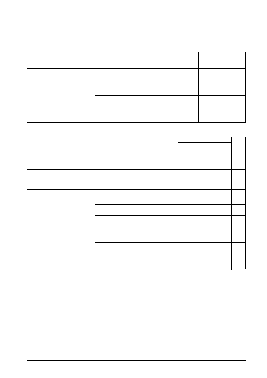
Parameter
Symbol
Conditions
Ratings
Unit
Maximum supply voltage
V
DD
max
≠0.3 to +4.0
V
Input voltage
V
IN
All input pins
≠0.3 to V
DD
+0.3
V
Output voltage
V
OUT
(1)
AOUT, PE, TU
≠0.3 to +15
V
V
OUT
(2)
All output pins except V
OUT
(1)
≠0.3 to V
DD
+ 0.3
V
I
OUT
(1)
PC, PD, PG, PH, EO
0 to 3
mA
I
OUT
(2)
PB
0 to 1
mA
Output current
I
OUT
(3)
AOUT, PE, TU
0 to 2
mA
I
OUT
(4)
S1 to S20
300
µA
I
OUT
(5)
COM1 to COM4
3
mA
Allowable power dissipation
Pdmax
Ta = ≠20 to +70∞C
300
mW
Operating temperature
Topr
≠20 to +70
∞C
Storage temperature
Tstg
≠45 to +125
∞C
Specifications
Absolute Maximum Ratings
at Ta = 25∞C, V
SS
= 0 V
Parameter
Symbol
Conditions
Ratings
Unit
min
typ
max
V
DD
(1)
PLL operating voltage
1.8
3.0
3.6
Supply voltage
V
DD
(2)
Memory retention voltage
1.0
V
V
DD
(3)
CPU operating voltage
1.4
3.0
3.6
V
DD
(4)
A/D converter operating voltage
1.6
3.0
3.6
V
IH
(1)
Input ports other than V
IH
(2), V
IH
(3), AMIN,
0.7 V
DD
V
DD
V
Input high-level voltage
FMIN, HCTR, and XIN
V
IH
(2)
BRES port
0.8 V
DD
V
DD
V
V
IH
(3)
Port PF
0.6 V
DD
V
DD
V
V
IL
(1)
Input ports other than V
IL
(2), V
IL
(3), AMIN,
0
0.3 V
DD
V
Input low-level voltage
FMIN, HCTR, and XIN
V
IL
(2)
BRES port
0
0.2 V
DD
V
V
IL
(3)
Port PF
0
0.2 V
DD
V
V
IN
(1)
XIN
0.5
0.6
Vrms
Input amplitude
V
IN
(2)
FMIN, AMIN
0.035
0.35
Vrms
V
IN
(3)
FMIN
0.05
0.35
Vrms
V
IN
(4)
HCTR
0.035
0.35
Vrms
Input voltage range
V
IN
(5)
ADIO, ADI1, ADI3
0
V
DD
V
F
IN
(1)
XIN: CI
35 k
70
75
80
kHz
F
IN
(2)
FMIN: V
IN
(2), V
DD
(1)
10
130
MHz
Input frequency
F
IN
(3)
FMIN: V
IN
(3), V
DD
(1)
130
250
MHz
F
IN
(4)
AMIN(H): V
IN
(2), V
DD
(1)
2
40
MHz
F
IN
(5)
AMIN(L): V
IN
(2), V
DD
(1)
0.5
10
MHz
F
IN
(6)
HCTR: V
IN
(4), V
DD
(1)
0.4
12
MHz
Allowable Operating Ranges
at Ta = ≠20 to +70∞C, V
DD
= 1.8 to 3.6 V
No. 7253-4/15
LC723481W/2W/3W
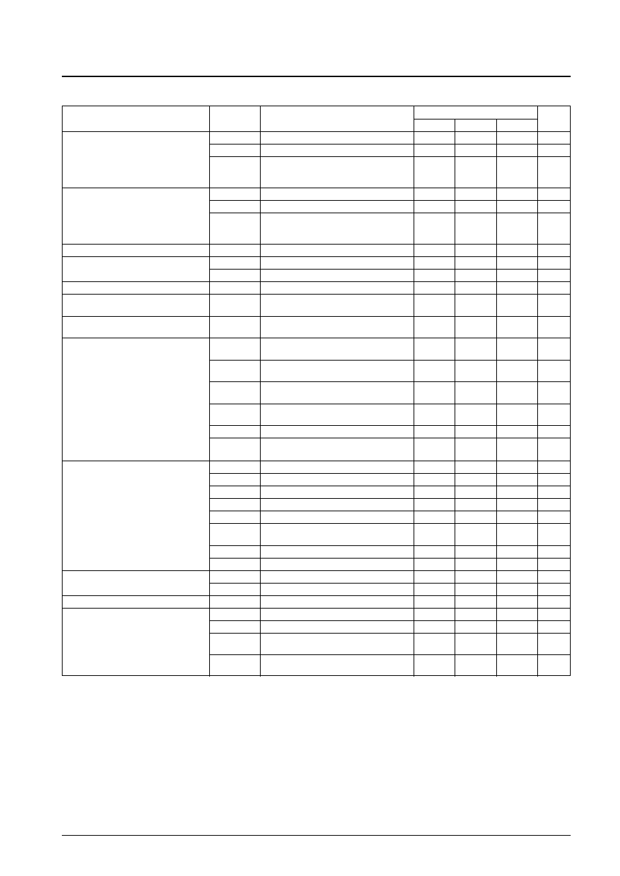
Parameter
Symbol
Conditions
Ratings
Unit
min
typ
max
I
IH
(1)
XIN: V
I
= V
DD
= 3.0 V
3
µA
Input high-level current
I
IH
(2)
FMIN, AMIN, HCTR: V
I
= V
DD
= 3.0 V
3
8
20
µA
PA/PF (without pull-down resistors), the PC,
I
IH
(3)
PD, PG, PH, ports,
3
µA
and BRES: V
I
= V
DD
= 3.0 V
I
IL
(1)
XIN: V
DD
= V
SS
≠3
µA
Input low-level current
I
IL
(2)
FMIN, AMIN, HCTR: V
I
= V
DD
= V
SS
≠3
≠8
≠20
µA
PA/PF (without pull-down resistors), the PC,
I
IL
(3)
PD, PG, PH, ports,
≠3
µA
and BRES: V
I
= V
DD
= V
SS
Input floating voltage
V
IF
PA/PF (with pull-down resistors)
0.05 V
DD
V
Pull-down resistor values
R
PD
(1)
PA/PF (with pull-down resistors), V
DD
= 3.0 V
75
100
200
k
R
PD
(2)
TEST1, TEST2
10
k
Hysteresis
V
H
BRES
0.1 V
DD
0.2 V
DD
V
Voltage doubler reference voltage
DBR4
Referenced to V
DD
, C(3) = 0.47 µF,
1.3
1.5
1.7
V
Ta = 25∞C
*
1
Voltage doubler step-up voltage
DBR1, 2, 3
C(1) = 0.47 µF
2.7
3.0
3.3
V
C(2) = 0.47 µF, without loading, Ta = 25∞C
*
1
V
OH
(1)
PB: I
O
= ≠1 mA
V
DD
≠
V
DD
≠
V
0.7 V
DD
0.3 V
DD
V
OH
(2)
PC, PD, PG, PH, : I
O
= ≠1 mA
V
DD
≠
V
0.3 V
DD
V
OH
(3)
EO: I
O
= ≠500 µA
V
DD
≠
V
Output high-level voltage
0.3 V
DD
V
OH
(4)
XOUT: I
O
= 200 µA
V
DD
≠
V
0.3 V
DD
V
OH
(5)
S1 to S20: I
O
= ≠20 µA
*
1
2.0
V
V
OH
(6)
COM1, COM2, COM3, COM4:
2.0
V
I
O
= ≠100 µA
*
1
V
OL
(1)
PB: I
O
= ≠50 µA
0.3 V
DD
0.7 V
DD
V
V
OL
(2)
PC, PD, PG, PH, PE: I
O
= ≠1 mA
0.3 V
DD
V
V
OL
(3)
EO: I
O
= ≠500 µA
0.3 V
DD
V
V
OL
(4)
XOUT: I
O
= ≠200 µA
0.3 V
DD
V
Output low-level voltage
V
OL
(5)
S1 to S20: I
O
= ≠20 µA
*
1
1.0
V
V
OL
(6)
COM1, COM2, COM3, COM4:
1.0
V
I
O
= ≠100 µA
*
1
V
OL
(7)
PE: I
O
= 2 mA
1.0
V
V
OL
(8)
AOUT (AIN = 1.3 V), TU: I
O
= 1 mA, V
DD
= 3 V
0.5
V
Output off leakage current
I
OFF
(1)
Ports PB, PC, PD, PG, PH and EO
≠3
+3
µA
I
OFF
(2)
AOUT, PE and port TU
≠100
+100
nA
A/D converter error
ADI0, ADI1, ADI3, V
DD
(4)
≠1/2
+1/2
LSB
I
DD
(1)
V
DD
(1): F
IN
(2) 130 MHz, Ta = 25∞C
5
mA
I
DD
(2)
V
DD
(2): In HALT mode, Ta = 25∞C
*
2
0.1
mA
Current drain
I
DD
(3)
V
DD
= 3.6 V, with the oscillator stopped,
1
µA
Ta = 25∞C
*
3
I
DD
(4)
V
DD
= 1.8 V, with the oscillator stopped,
0.5
µA
Ta = 25∞C
*
3
Electrical Characteristics
within the allowable operating ranges
Note: The halt mode current is due to the CPU executing 20 instruction steps every 125 ms.
Note: * C(1), C(2), and C(3) must be connected even if an LCD is not used.
No. 7253-5/15
LC723481W/2W/3W
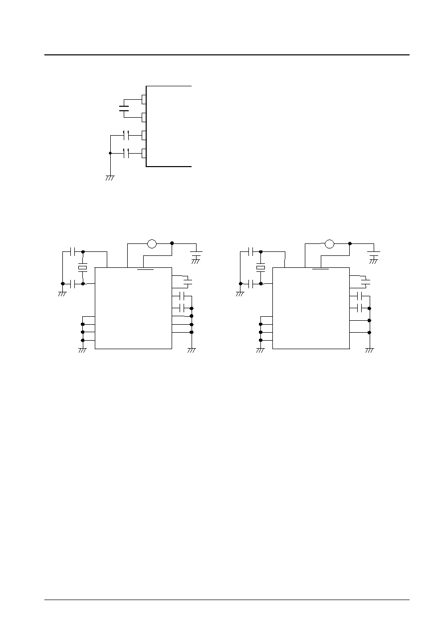
DBR1
DBR2
DBR3
0.1 to 1
µ
F
0.1 to 1
µ
F
0.1 to 1
µ
F
C(C1)
C(C2)
DBR4
C(C3)
Notes: *1. The capacitors C(1), C(2), and C(3) must be connected to the DBR pins.
A
A
7 pF
7 pF
FMIN
XIN
AMIN
TEST1, 2
HCTR
XOUT VDD
DBR2
DBR1
DBR1
0.1
µ
F
0.1
µ
F
0.1
µ
F
0.1
µ
F
0.1
µ
F
0.1
µ
F
DBR3
DBR4
BRES
BRES
VSS
PA, PF
AIN
FMIN
XIN
AMIN
TEST1, 2
HCTR
XOUT VDD
VSS
AIN
7pF
75 kHz
75 kHz
7pF
DBR2
DBR3
DBR4
*2. Halt mode current measurement circuit
*3. Backup mode current measurement circuit
With all ports other than those specified above left open.
With output mode selected for PC and PD.
With segments S13 to S20 selected.
With all ports other than those specified above left open.
With output mode selected for PC and PD.
With segments S13 to S20 selected.