 | –≠–ª–µ–∫—Ç—Ä–æ–Ω–Ω—ã–π –∫–æ–º–ø–æ–Ω–µ–Ω—Ç: LC7265 | –°–∫–∞—á–∞—Ç—å:  PDF PDF  ZIP ZIP |
Received Frequency Display for Radio Receivers
Features
.
Displays received frequency of each band of FM, MW, LW
(LED static display).
.
Counts local oscillation frequency and displays received
frequency.
.
Number of display digits : FM-5 digits, MW-4 digits, LW-3
digits.
.
Covers intermediate frequencies shown below.
FM :
+10.700, +10.725, +10.750, +10.675 MHz
≠10.700, ≠10.725, ≠10.675, ≠10.650 MHz
MW, LW :
+450 kHz : 10 kHz step display
+450 kHz : 1 kHz step display
+455 kHz : 1 kHz step display
+469 kHz : 1 kHz step display
.
Contains blanking circuit to turn off display.
.
Contains hold circuit to hold display contents.
.
Uses crystal resonator having 7.2 MHz reference frequency.
.
Uses LB3500 (
˜
8 prescaler) jointly at the time of FM
reception.
.
Supply voltage V
DD
: 4.5 V to 10 V
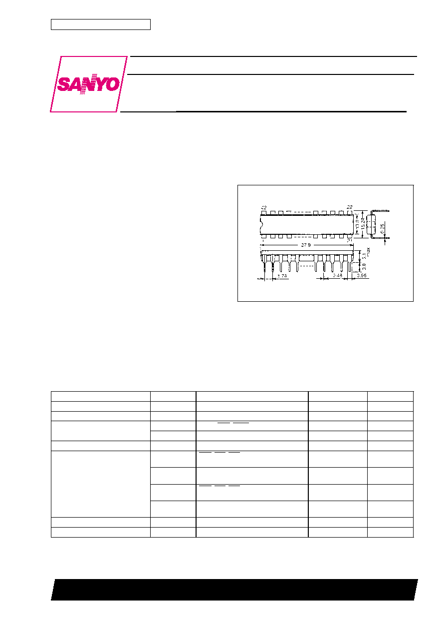
Package Dimensions
unit : mm
3025B-DIP42S
[LC7265]
SANYO : DIP42S
Specifications
Absolute Maximum Ratings
at Ta = 25 ∞C, V
SS
= 0 V
Parameter
Symbol
Conditions
Ratings
Unit
Maximum supply voltage
V
DD
max
≠0.3 to +11
V
Input voltage
V
IN
All input pins
≠0.3 to V
DD
+0.3
V
Output voltage
V
O
1
X
OUT
, HLD, 50 Hz, output: off
≠0.3 to V
DD
+0.3
V
V
O
2
Output pins other than V
O
1
0 to 15
V
Allowable power dissipation
Pd max
Ta
%
65 ∞C
550
mW
Allowable power dissipation of
segment outputs
Pd (seg)1
MHz, b&c, b&e, V
DD
= 4.5 to 6.5 V,
I
OL
= 33 mA
30
mW
Pd (seg) 2
Other outputs, V
DD
= 4.5 to 6.5 V,
I
OL
= 16.5 mA
15
mW
Pd (seg) 3
MHz, b&c, b&e, V
DD
= 6.0 to 10 V,
I
OL
= 36 mA
25
mW
Pd (seg) 4
Other outputs, V
DD
= 6.0 to 10 V,
I
OL
= 18 mA
12
mW
Operating temperature
Topr
≠30 to +65
∞C
Storage temperature
Tstg
≠40 to +125
∞C
Ordering number: EN 1197F
CMOS IC
LC7265
SANYO Electric Co.,Ltd. Semiconductor Bussiness Headquarters
TOKYO OFFICE Tokyo Bldg., 1-10, 1 Chome, Ueno, Taito-ku, TOKYO, 110-8534 JAPAN
63098HA(II)/6088YT/9105KI/3173KI/D162KI/7162KI/6242KI,TS No.1197-1/6
Allowable Operating Ranges
at Ta = 25 ∞C, V
DD
= 4.5 to 10 V, V
SS
= 0 V
Parameter
Symbol
Conditions
min
typ
max
Unit
Supply voltage
V
DD
4.5
10
V
Input high-level voltage
V
IH
1
A/F, BLK
0.7V
DD
V
DD
V
V
IH
2
FIF1, FIF2, FIF3, AIF1, AIF2
0.9V
DD
V
DD
V
Input low-level voltage
V
IL
1
A/F, BLK
0
0.3V
DD
V
V
IL
2
FIF1, FIF2, FIF3, AIF1, AIF2
0
0.1V
DD
V
Input frequency
f
IN
1
FMI, sine wave, capacitive coupling,
V
IN
1 = 0.7Vp-p
1
18
MHz
f
IN
2
AMI, sine wave, capacitive coupling,
V
IN
2 = 0.5Vp-p*
0.5
3
MHz
f
IN
3
X
IN
0.2
7.5
MHz
Input amplitude
V
IN
1
FMI, sine wave, capacitive coupling,
f
IN
1 = 1 to 18 MHz
0.7
0.9V
DD
Vp-p
V
IN
2
AMI, sine wave, capacitive coupling,
f
IN
2 = 0.5 to 3 MHz
0.5*
0.9V
DD
Vp-p
V
IN
3
X
IN
, sine wave, capacitive coupling,
f
IN
3 = 0.2 to 7.5 MHz
1.0
0.9V
DD
Vp-p
Segment current
Iseg1
MHz, b&e, b&c
0
30
mA
Iseg2
Other outputs
0
15
mA
*: For f
IN
2 = 0.5 MHz to 0.9 MHz and V
DD
= 8 to 10 V, V
IN
2 min = 1.0 Vp-p applies.
Electrical Characteristics
at Ta = 25 ∞C, V
DD
= 4.5 to 10 V, V
SS
= 0 V
Parameter
Symbol
Conditions
min
typ
max
Unit
Input high-level current
I
IH
1
FIF1, FIF2, FIF3, AIF1, AIF2
V
I
= V
DD
0
10
µA
I
IH
2
BLK
V
I
= V
DD
0
2
µA
Input low-level current
I
IL
1
FIF1, FIF2, FIF3, AIF1, AIF2
V
I
= V
SS
0
10
µA
I
IL
2
BLK
V
I
= V
SS
0
2
µA
I
IL
3
A/F
V
I
= V
SS
20
500
µA
Input floating voltage
V
IF
A/F
V
I
= open
0.8V
DD
V
DD
V
Input/output high-level leakage
current
I
OFF
HLD, output off, V
I
= V
DD
0
2
µA
Output low-level voltage
V
OL
1
HLD, output on, I
O
= 1 mA
0
1
V
V
OL
2
b&e, b&c, MHz V
DD
= 4.5 to 10 V,
I
OL
= 30 mA
0
0.7
V
V
OL
3
Segments other than above
V
DD
= 4.5 to 10 V, I
OL
= 15 mA
0
0.7
V
V
OL
4
50 Hz, I
O
= 0.2 mA
0
1.0
V
Input high-level threshold voltage
Vth
HLD
0.4V
DD
0.5V
DD
0.7V
DD
V
Output off leakage current
I
OFF
2
All segments output pins, V
O
= 13 V, output off
0
10
µA
Current drain
I
DD
FM mode, A/F = open or V
DD
, f
IN
1 = 18 MHz,
0.7Vp-p or (AM mode, A/F = V
SS
, f
IN
2 =
3 MHz, 0.5Vp-p) f
IN
3 = 7.2 MHz, 1Vp-p
FIF1, FIF2, FIF3 = V
DD
AIF1, AIF2 = V
DD
HLD, BLK = V
DD
other pins open
0
18
mA
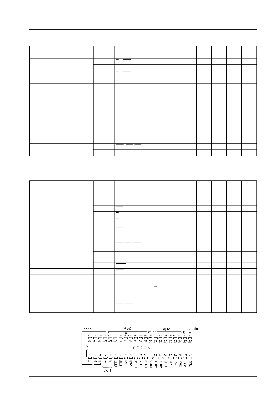
Pin Assignment
Top view
LC7265
No.1197-2/6
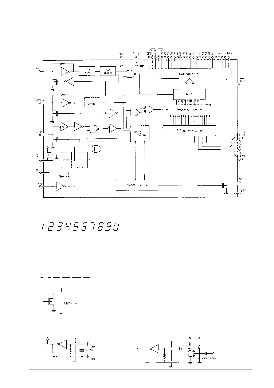
Equivalent Circuit Block Diagram
1. Display
1-1 Display font
1-2 Lighting system
.
Static lighting
1-3 Display range (High-order 1 digit : zero blanking)
.
FM
: 00.00 MHz to 199.95 MHz
50 kHz step
.
MW, LW
: 000 kHz to 1999 kHz
10 kHz or 1 kHz step
2. Pin Description
2-1
.
a to g, b&c, b&e, MHz, kHz : LED
2-2
.
V
DD
, V
SS
: Power supply pins
2-3
.
X
IN
, X
OUT
: Crystal resonator or input amp pin
LC7265
No.1197-3/6
2-4
.
FIF1, FIF2, FIF3 : FM IF select pins
FIF1
0
0
0
0
1
1
1
1
FIF2
0
0
1
1
0
0
1
1
FIF3
0
1
0
1
0
1
0
1
IF (MHz)
+10.700
+10.725
+10.675
+10.750
≠10.700
≠10.725
≠10.675
≠10.650
2-5
.
AIF1, AIF2 : AM IF select pins
AIF1
0
0
1
1
AIF2
0
1
0
1
IF (kHz)
+450 (2)
+450 (1)
+455
+469
(Note) 450 kHz(1) : 10 kHz step display, others : 1 kHz step display
1 : High level (V
DD
)
0 : Low level (V
SS
)
2-6
.
HLD : Display contents hold pin
Normally, this pin is set at high level. To hold display contents, this pin is set at low level. Connecting time constant circuit
to this pin makes it possible to hold display contents for a certain period of time at the time of FM/MW, LW band
selection.
2-7
.
BLK : Display blanking pin
2-8
.
FMI, AMI : Local oscillation signal input pins
FMI -- For FM
: 0.7Vp-p input sensitivity
AMI -- For MW, LW : 1.0Vp-p input sensitivity (V
DD
= 8 to 10 V, f
IN
= 0.5 to 0.9 MHz)
0.5Vp-p input sensitivity (other than above)
2-9
.
A/F : FM/MW, LW select pin
FM
-- Pin open or high level
MW, LW -- Low level
2-10
.
50 Hz : 50 Hz time base output pin
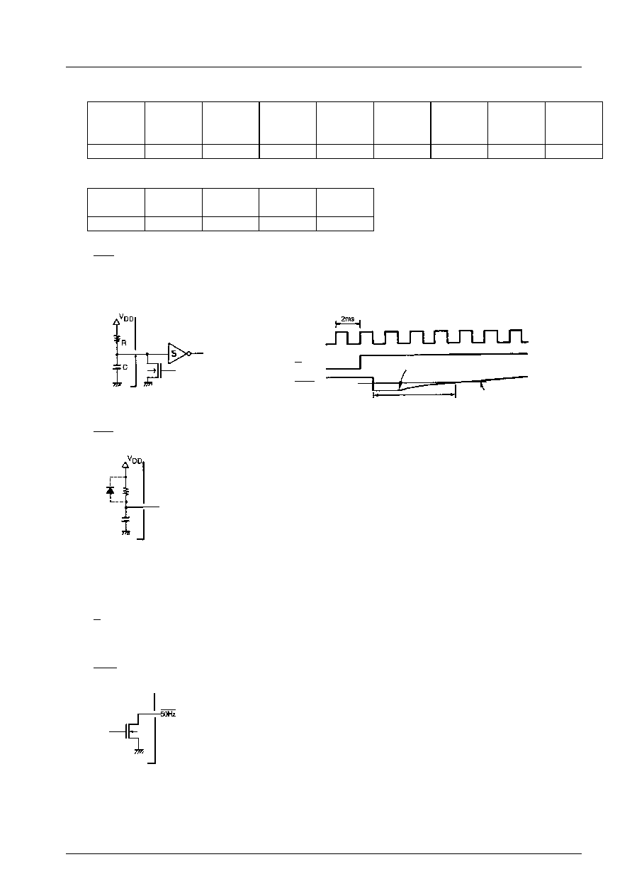
Internal clock
Depending on C, R
Display contents hold
Threshold
voltage of
e
HLD
A/F
Example of blanking misdisplay
at the time of application of power.
LC7265
No.1197-4/6
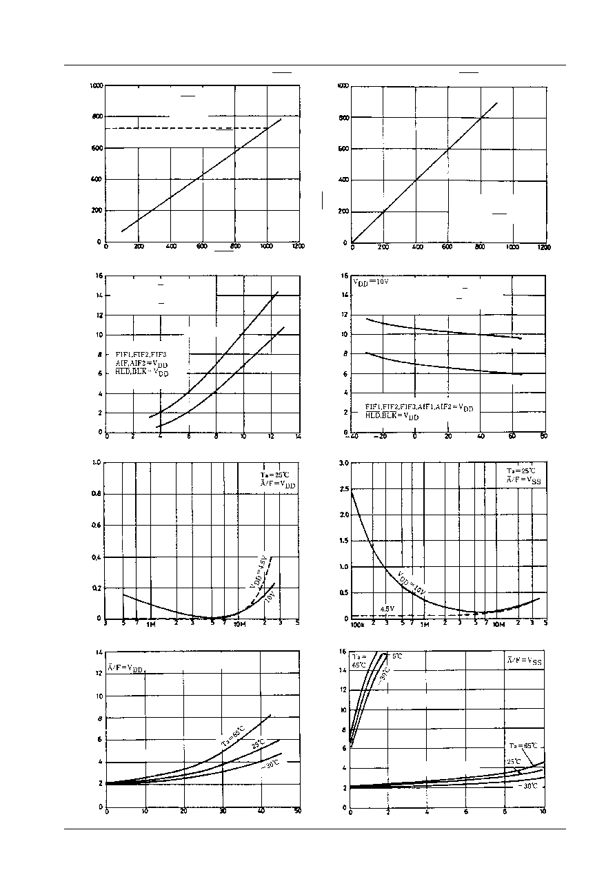
Hold
time
≠
m
s
Hold time ≠ time constant connected to HLD pin
To obtain 1-s hold time make time
constant connected to HLD pin 720 ms.
C = 2.2 µF
R = 470 k
Note: time constant connected to HLD
pin must be 100 ms or more.
Time constant connected to HLD pin, (t = CR) ≠ ms
T
ime
constant
connected
to
BLK
pin
(t
=
CR)
≠
m
s
Time constant connected to BLK pin - V
DD
rise time
If VDD rise time is 200 ms,
make time constant externally
connected to BLK pin 200 ms
or more.
C = 1 µF
R = 200 k
or more
V
DD
rise time ≠ ms
Current
drain,
I
DD
≠m
A
For FMI input : 18 MHz, 0.7Vp-p,
A/F = VDD
For AMI input : 3 MHz, 0.5Vp-p,
A/F = VSS
Common conditions
Other pins open
For FMI input
For AMI input
Supply voltage, V
DD
≠ V
Current
drain,
I
DD
≠m
A
I
DD
≠ Ta
For FMI input : 18 MHz, 0.7Vp-p, A/F = VDD
For AMI input : 3 MHz, 0.5Vp-p,A/F = VSS
For FMI input
For AMI input
Common conditions
Other pins open
Ambient temperature, Ta ≠ ∞C
I
DD
≠ V
DD
Input
amplitude
≠
mVp-p
Vp-p ≠ f
IN
1
FMI input frequency, f
IN
1 ≠ Hz
Input
amplitude
≠
mVp-p
Vp-p ≠ f
IN
2
AMI input frequency, f
IN
2 ≠ Hz
Supply
voltage,
V
DD
≠V
V
DD
≠ f
IN
1
Upper standard value. V
DD
= 15 V or more
Lower standard value
FMI input frequency, f
IN
1 ≠ MHz
Supply
voltage,
V
DD
≠V
V
DD
≠ f
IN
2
Upper standard value
Lower standard value
AMI input frequency, f
IN
2 ≠ MHz
LC7265
No.1197-5/6
No products described or contained herein are intended for use in surgical implants, life-support systems, aerospace equipment,
nuclear power control systems, vehicles, disaster/crime-prevention equipment and the like, the failure of which may directly or
indirectly cause injury, death or property loss.
Anyone purchasing any products described or contained herein for an above-mentioned use shall:
1
Accept full responsibility and indemnify and defend SANYO ELECTRIC CO., LTD., its affiliates, subsidiaries and distributors
and all their officers and employees, jointly and severally, against any and all claims and litigation and all damages, cost and
expenses associated with such use:
2
Not impose any responsibility for any fault or negligence which may be cited in any such claim or litigation on SANYO
ELECTRIC CO., LTD., its affiliates, subsidiaries and distributors or any of their officers and employees jointly or severally.
Information (including circuit diagrams and circuit parameters) herein is for example only; it is not guaranteed for volume
production. SANYO believes information herein is accurate and reliable, but no guarantees are made or implied regarding its use
or any infringements of intellectual property rights or other rights of third parties.
This catalog provides information as of June, 1998. Specifications and information herein are subject to change without notice.
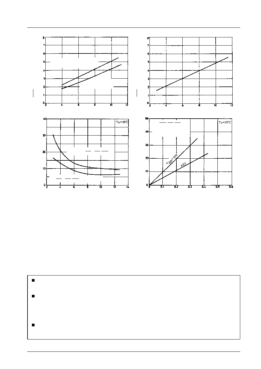
HLD
threshold
voltage,
V
t
≠V
V
t
≠ V
DD
Upper standard value
high-level threshold voltage
Lower standard value
low-level threshold voltage
Supply voltage, V
DD
≠ V
BLK
threshold
voltage,
V
t
≠V
V
t
≠ V
DD
Supply voltage, V
DD
≠ V
Output
impedance,
R
OUT
≠
R
OUT
≠ V
DD
Segment outputs (IOL = 15 mA)
other than 5b&e, 1b&c, MHz
Segment outputs (IOL = 30 mA)
of 5b&e, 1b&c, MHz
Supply voltage, V
DD
≠ V
Output
current,
I
OL
≠m
A
I
OL
≠ V
OL
Segment outputs other
than MHz, b&c, b&e
This data is in case of
flowing current to one
segment only.
Output voltage, V
OL
≠ V
LC7265
No.1197-6/6