 | –≠–ª–µ–∫—Ç—Ä–æ–Ω–Ω—ã–π –∫–æ–º–ø–æ–Ω–µ–Ω—Ç: LC7267 | –°–∫–∞—á–∞—Ç—å:  PDF PDF  ZIP ZIP |
Digital Display of Clock/Receiving Frequency
for Radio Set Applications
Functions
.
Capable of selecting receiving frequency display/time
display.
.
Display of receiving frequency at each band of FM/MW/LW
Display element:
LED
Static/dynamic:
Static
Withstand voltage at output pin: 15 V
Maximum current:
18 mA
(V
DD
= 6.0 to 10.0 V)
.
Number of display digits:
FM: 5 digits, MW, LW: 4 digits
.
Covers intermediate frequencies shown below.
FM:
+10.700, +10.725, +10.750, +10.675 MHz
≠10.700, ≠10.725, ≠10.675, ≠10.650 MHz
MW, LW:
+450 kHz (1) : 10 kHz-step display
+450 kHz (2) : 1 kHz-step display
+455 kHz
: 1 kHz-step display
+469 kHz
: 1 kHz-step display
.
In FM reception applications, the LB3500 (
˜
8 prescaler) is
used jointly.
.
Two selections of display system (12-hour system with PM
sign, 24-hour system).
.
Easy to set time by the time signal.
.
Inhibit pin for inhibiting time setting with display unlighted.
.
7.2 MHz crystal oscillator for reference frequency.
.
Supply voltage V
DD
: 4.5 to 10.0 V.
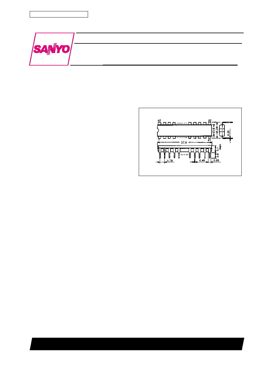
Package Dimensions
unit : mm
3025B-DIP42S
[LC7267]
SANYO : DIP42S
Ordering number: EN 1511B
CMOS IC
LC7267
SANYO Electric Co.,Ltd. Semiconductor Bussiness Headquarters
TOKYO OFFICE Tokyo Bldg., 1-10, 1 Chome, Ueno, Taito-ku, TOKYO, 110-8534 JAPAN
63098HA (II) No.1511 - 1/10
Specifications
Absolute Maximum Ratings
at V
SS
= 0 V
Parameter
Symbol
Conditions
Ratings
Unit
Maximum supply voltage
V
DD
max
≠0.3 to +11
V
Input voltage
V
IN
≠0.3 to V
DD
+0.3
V
Output voltage
V
O
1
X
OUT
≠0.3 to V
DD
+0.3
V
V
O
2
Output pins other than X
OUT
, output : off
0 to 15
V
Allowable power
dissipation
Pd max
Ta
%
65∞C
550
mW
Allowable power
dissipation of segment
outputs
Pd seg 1
PM V
DD
= 4.5 to 6 V, I
OL
= 50 mA
35
mW
Pd seg 2
b&e V
DD
= 4.5 to 6 V, I
OL
= 33 mA
30
mW
Pd seg 3
Other outputs V
DD
= 4.5 to 6.5 V,
I
OL
= 16.5 mA
15
mW
Pd seg 4
PM V
DD
= 6.0 to 10 V, I
OL
= 54 mA
38
mW
Pd seg 5
b&e V
DD
= 6.0 to 10 V, I
OL
= 36 mA
25
mW
Pd seg 6
Other outputs V
DD
= 6.0 to 10 V,
I
OL
= 18 mA
13
mW
Operating temperature
Topr
≠30 to +65
∞C
Storage temperature
Tstg
≠40 to +125
∞C
Allowable Operating Conditions
at Ta = 25∞C, V
SS
= 0 V, V
DD
= 4.5 to 10 V
Parameter
Symbol
Conditions
min
typ
max
Unit
Supply voltage
V
DD
4.5
10
V
Input high-level voltage
V
IH
1
INHI, CTR/CLK, DEMAND
0.8V
DD
V
DD
V
V
IH
2
SET, FM/AM
0.85V
DD
V
DD
V
V
IH
3
FIF1, FIF2, FIF3
AIF1, AIF2, 12H/24H
0.9V
DD
V
DD
V
Input low-level voltage
V
IL
1
INHI, CTR/CLK, DEMAND
0
0.2V
DD
V
V
IL
2
SET, FM/AM
0
0.15V
DD
V
V
IL
3
FIF1, FIF2, FIF3
AIF1, AIF2, 12H/24H
0
0.1V
DD
V
Input medium-level
voltage
V
IM
SET
0.45V
DD
0.55V
DD
V
Input frequency
f
IN
1
FMI, sine wave, capacitive coupling, V
IN
1 = 0.7Vp-p
1
18
MHz
f
IN
2
AMI, sine wave, capacitive coupling, V
IN
2 = 0.5Vp-p
0.5
3
MHz
f
IN
3
XIN, sine wave, capacitive coupling, V
IN
3 = 1Vp-p
0.2
7.5
MHz
Input amplitude
V
IN
1
FMI, sine wave, capacitive coupling,
f
IN
1 = 1 to 18 MHz
0.7
0.9V
DD
Vp-p
V
IN
2
AMI, sine wave, capacitive coupling,
f
IN
2 = 0.5 to 3 MHz
0.5
0.9V
DD
Vp-p
V
IN
3
XIN, sine wave, capacitive coupling,
f
IN
3 = 0.2 to 7.5 MHz
1.0
0.9V
DD
Vp-p
Segment current
Iseg 1
PM
45
mA
Iseg 2
b&e
30
mA
Iseg 3
Other outputs seg
15
mA
Electrical Characteristics
at V
DD
= 4.5 to 10 V, V
SS
= 0 V
Parameter
Symbol
Conditions
min
typ
max
Unit
Input high-level current
I
IH
1
FIF1 to FIF3, AIF1 to AIF2, SET, FM/AM, 12H/24H
CTR/CLK, V
I
= V
DD
0
10
µA
I
IH
2
INHI, V
I
= V
SS
40
1000
µA
I
IH
3
DEMAND, V
I
= V
DD
40
1000
µA
Input low-level current
I
IL
FIF1 to FIF3, AIF1 to AIF2, SET, FM/AM, 12H/24H,
CTR/CLK, V
I
= V
SS
≠10
0
µA
Input floating voltage
V
IF
1
INHI, V
I
= open
0
0.2
V
V
IF
2
DEMAND, V
I
= open
0
0.1V
DD
V
Continued next page.
LC7267
No. 1511- 2/10
Continued from preceding page.
Parameter
Symbol
Conditions
min
typ
max
Unit
Output low-level voltage
V
OL
1
PM V
DD
= 4.5 to 10 V, I
OL
= 45 mA
0
1.0
V
V
OL
2
b&e V
DD
= 4.5 to 10 V, I
OL
= 30 mA
0
1.0
V
V
OL
3
Other outputs seg, V
DD
= 4.5 to 10 V, I
OL
= 15 mA
0
1.0
V
Output off leakage current
I
OFF
All segments output pins, V
OUT
= 13 V
0
10
µA
Current drain
I
DD
FM mode, FM/AM = V
DD
, f
IN
1 = 18 MHz, 0.7Vp-p
(or AM mode, FM/AM = V
SS
, f
IN
2 = 3 MHz, 0.5Vp-p)
f
IN
3 = 7.2 MHz, 1Vp-p,
FIF1, FIF2, FIF3 = V
DD
AIF1, AIF2 = V
DD
12H/24H, CTR/CLK, INHI, DEMAND = V
DD
18
mA
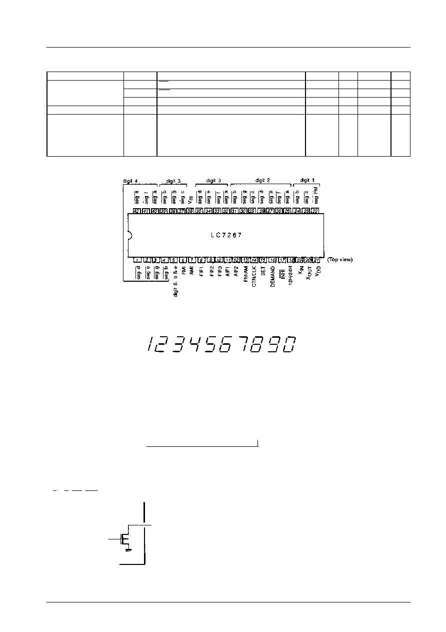
Pin Assignment
Configuration and Display Font
4 or 4-1/2-digit segment LED's are used to display time and frequency in the display font shown below.
Lighting System
Static lighting
Display Range
.
Frequency (MW, LW)
000 kHz to 1999 kHz (The highest-order digit ``0'' is blanked out.)
.
Frequency (FM)
00.00 MHz to 199.95 MHz (The highest-order digit ``0'' is blanked out.)
.
Clock (12-hour)
PM 12:00 to PM 11:59
12:00 to 11:59
.
Clock (24-hour)
0:00 to 23:59 (The highest-order digit ``0'' is blanked out.)
Pin Description
.
a to g, PM, b&e: LED driver pin
Font
LC7267
No. 1511- 3/10
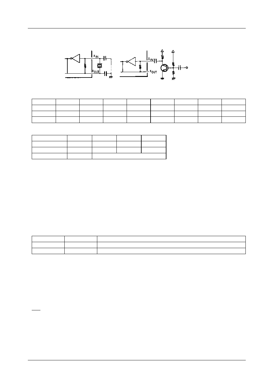
.
V
DD
, V
SS
:
Power supply pin
.
X
IN
, X
OUT
:
Crystal oscillator, input amplifier pin
.
FIF1, FIF2, FIF3: FM IF offset value select pin
FIF1
0
0
0
0
1
1
1
1
FIF2
0
0
1
1
0
0
1
1
FIF3
0
1
0
1
0
1
0
1
IF (MHz)
+10.700
+10.725
+10.675
+10.750
≠10.700
≠10.725
≠10.675
≠10.650
.
AIF1, AIF2: AM IF offset value select pin
AIF1
0
0
1
1
AIF2
1
0
0
1
IF (kHz)
+450 (1)
+450 (2)
+455
+469
Display step
10 kHz
1 kHz step
1: High level
0: Low level
(Note) 450 kHz (1): 10 kHz-step display, others: 1 kHz-step display
.
FMI, AMI: Local OSC signal input pin
FMI: For FM
AMI: For MW, LW
.
FM/AM:
FM/MW, LW select pin
FM:
High level
MW, LW: Low level
.
CTR/CLK: Frequency display/time display select pin
CTR (Counter): High level
CLK (Clock):
Low level
.
DEMAND: Input pin for instructing execution of setting
CTR/CLK
DEMAND
MODE
0
1
Mode of setting by the time signal and hours-minutes setting mode
0
0
Time display mode
.
SET:
Input pin for setting hours-minutes
This pin is set at ``M'' level normally. The input signal of ``H''/``L'' level acts as follows:
When in the mode of setting by the time signal and hours-minutes setting mode (CTR/CLK = ``L'', DEMAND = ``H'')
High level: Execution of hours setting
Advance at a 2 Hz rate 1.2 seconds after the pin is set to ``H'' level.
Low level: Execution of setting by the time signal and minutes setting
Advance at a 2 Hz rate 1.2 seconds after the pin is set to ``L'' level.
Setting by the time signal is executed when the pin is set off within 1.0 second after set to ``L'' level.
No carry to high-order digit occurs.
.
INHI:
Input pin for turning OFF the segment pins, inhibiting the SET/DEMAND pin from functioning, and preventing the
AMI amp from operating
High level: Normal operation
Low level: Segment pin OFF, SET/DEMAND pin function inhibit
.
12H/24H: Input pin for selecting 12-hour system with PM sign/24-hour system
High level: 12-hour system with PM sign
Low level: 24-hour system
Crystal oscillator
Input amplifier
LC7267
No. 1511- 4/10
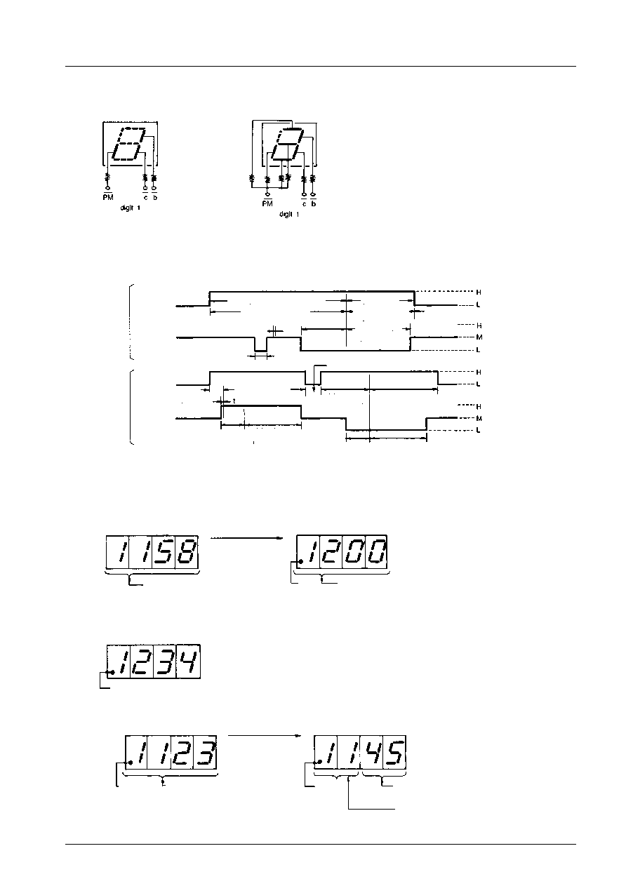
Make connection of the highest-order digit as shown below.
Timing Chart
Time setting (CTR/CLK = ``L'')
Sample Display at Each Display
(Setting by the time signal, hours-minutes display, hours-minutes setting)
Setting by the time signal: Setting to PM 12:00
Hours-minutes display: Display of PM 12:34
Hours-minutes setting: Setting to PM 11:45 from PM 11:23
12-hour system
24-hour system
Setting by the
time signal and
minutes setting
DEMAND pin
Flashing (2Hz) for setting by
the time signal
Mode of setting by
the time signal
Flashing stop
Hours-minutes
setting mode
Minutes
advance at
a 2 Hz rate
Hours-minutes
display
1.2 s. or more
Execution of counting
30min. or more as 1hr.
and disregarding 29min. or less
SET pin
Within 1.0 s.
Hours-minutes display
Hours setting
and minutes
setting
DEMAND pin
Flashing (2 Hz)
for setting by
the time signal
SET pin
(Hours setting)
Hours-minutes
setting mode
Flashing stop
1.2s
t: Approximately 100 ms.
Flashing (2 Hz)
for setting by
the time signal
Hours-minutes
setting mode
Flashing stop
Execution of minutes
setting
(Advance at a 2 Hz rate)
1.2s
Execution of hours
setting
(Advance at a 2 Hz rate)
Execute setting by
the time signal with
the SET pin.
Flashing at a 2 Hz rate when in
the mode of setting by the time
signal
PM
sign
When setting by the time signal is
executed, minutes become 00. If the
minutes display is at 30 to 59, hours are
incremented by 1 (counting 30 or more
as 1 hr. and disregarding 29 or less).
Flashing at a 2 Hz rate
The PM sign flashes in the afternoon when in the mode of
setting by the time signal, hours-minutes display,
hours-minutes setting.
(for 12-hour system).
PM sign
Set the SET pin to
V
DD
or V
SS
.
After
lapse of 1.2 s,
flashing stops and
hours or minutes
advance at a 2 Hz
rate.
PM sign
Flashing at
a 2 Hz rate
PM
sign
Set the SET pin to V
SS
,
and
setting is executed.
Set the SET pin to V
DD
,
and
setting is executed.
LC7267
No. 1511- 5/10
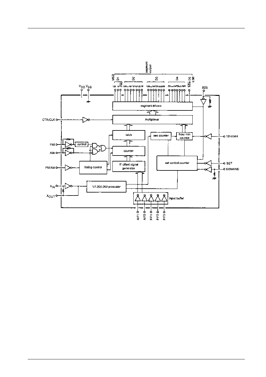
Equivalent Circuit Block Diagram
LC7267
No. 1511- 6/10
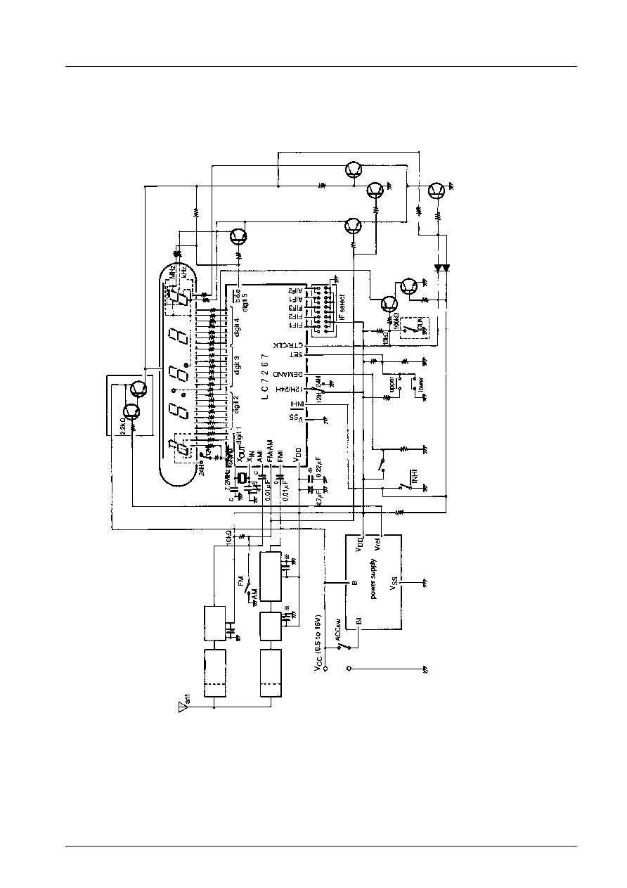
Sample Application Circuit 1
5-digit display in FM use
Surge
voltage
eliminator
LED
display
tube
(anode
common)
AM
local
Interface
FM/AM
display
select
SW
FM
local
Inter-
face
1/8
prescaler
LB3500
Hours-
minutes
setting
SW
*:
Ceramic
capacitor
(Must
be
mounted
as
close
to
each
pin
as
possible.)
LC7267
No. 1511- 7/10
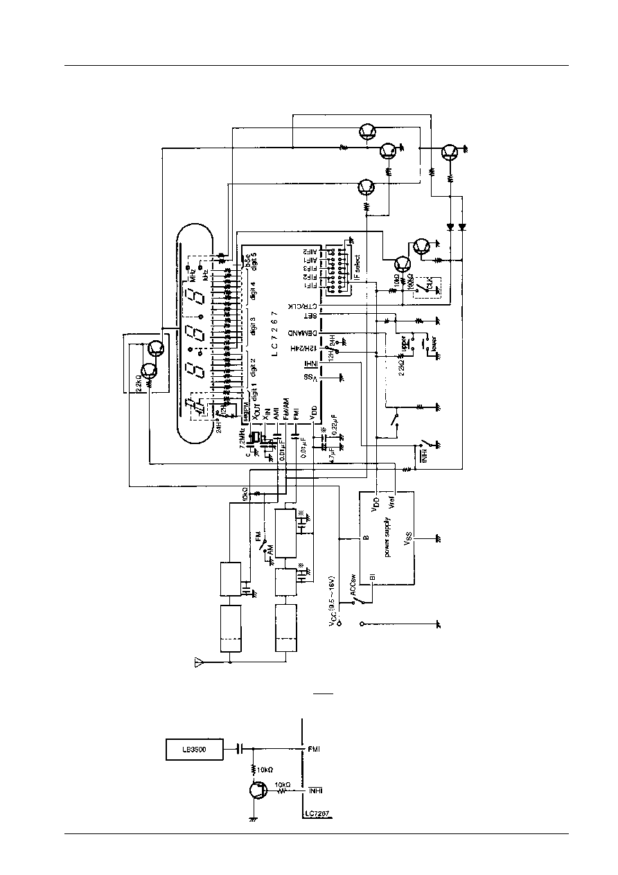
Sample Application Circuit 2
4-digit display in FM use
(Note) How to reduce current dissipation when display is turned off
To reduce current dissipation when display is turned off (INHI: ``L''), the circuit shown below must be connected to the
FMI pin.
Surge
voltage
eliminator
Reference:
LED
display
tube
(For
details,
see
LED
catalog.)
LED
display
tube
(anode
common)
AM
local
Interface
FM/AM
display
select
SW
FM
local
Inter-
face
1/8
prescaler
LB3500
Hours-
minutes
setting
SW
*:
Ceramic
capacitor
(Must
be
mounted
as
close
to
each
pin
as
possible.)
LC7267
No. 1511- 8/10
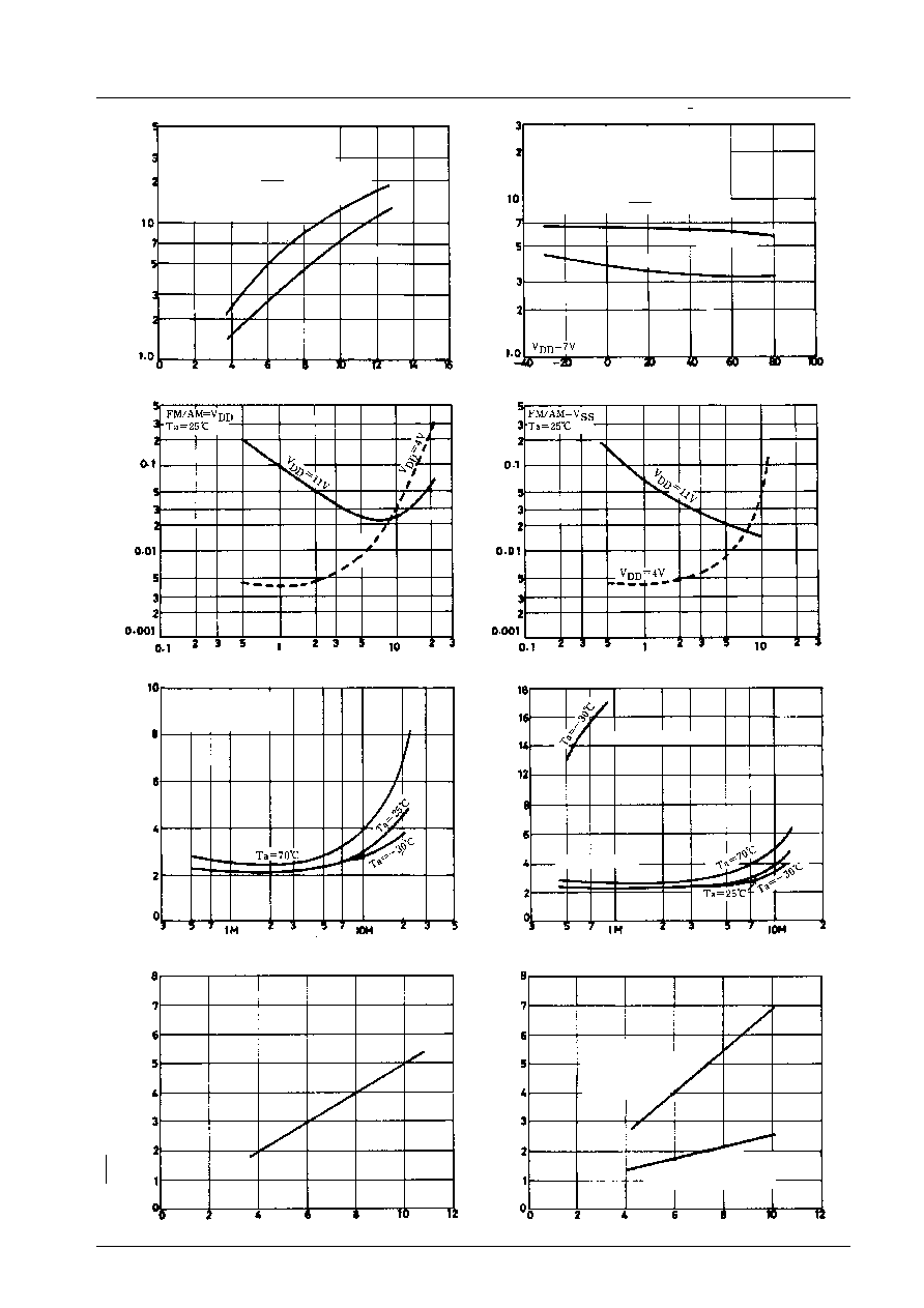
Current
drain,
I
DD
≠m
A
For FMI input: 18 MHz,
0.7 Vp-p FM/AM = ``H''
For AMI input: 3 MHz,
0.5 Vp-p FM/AM = ``L''
Common conditions
12H/24H, CTR/CLK, INHI, DEMAND = V
DD
FIF1, FIF2, FIF3 = VDD
AIF1, AIF2 = VDD For FMI input
For AMI input
Supply voltage, V
DD
≠ V
For FMI input: 18 MHz,
0.7 Vp-p FM/AM = ``H''
For AMI input: 3 MHz,
0.5 Vp-p FM/AM = ``L''
I
DD
≠ Ta
Common conditions
FIF1, FIF2, FIF3 = V
DD
AIF1, AIF2 = V
DD
12H/24H, CTR/CLK, INHI, DEMAND = V
DD
Current
drain,
I
DD
≠m
A
For FMI input
For AMI input
Ambient temperature, Ta ≠ ∞C
I
DD
≠ V
DD
Input
amplitude,
Vp-p
≠
FMI input frequency, f
I1
≠ Hz
Input
amplitude,
Vp-p
≠
AMI input frequency, f
I2
≠ Hz
Vp-p ≠ f
I1
Vp-p ≠ f
I2
FM/AM = V
DD
Upper standard value
V
DD
= 15 V or more
Supply
voltage,
V
DD
≠V
FMI input frequency, f
I1
≠ Hz
Supply
voltage,
V
DD
≠V
Upper standard value
Lower standard value
AMI Input Frequency, f
I2
≠ Hz
V
DD
≠ f
I1
V
DD
≠ f
I2
INHI
threshold
voltage,
V
t
≠V
Supply voltage, V
DD
≠ V
SET
threshold
voltage,
V
t
≠V
High-level
threshold voltage
Upper standard
value
Lower standard value
Low-level threshold voltage
Supply Voltage, V
DD
≠V
Vt ≠ V
DD
Vt ≠ V
DD
LC7267
No. 1511- 9/10
No products described or contained herein are intended for use in surgical implants, life-support systems,
aerospace equipment, nuclear power control systems, vehicles, disaster/crime-prevention equipment and the like,
the failure of which may directly or indirectly cause injury, death or property loss.
Anyone purchasing any products described or contained herein for an above-mentioned use shall:
1
Accept full responsibility and indemnify and defend SANYO ELECTRIC CO., LTD., its affiliates, subsidiaries and
distributors and all their officers and employees, jointly and severally, against any and all claims and litigation
and all damages, cost and expenses associated with such use:
2
Not impose any responsibility for any fault or negligence which may be cited in any such claim or litigation on
SANYO ELECTRIC CO., LTD., its affiliates, subsidiaries and distributors or any of their officers and employees
jointly or severally.
Information (including circuit diagrams and circuit parameters) herein is for example only; it is not guaranteed for
volume production. SANYO believes information herein is accurate and reliable, but no guarantees are made or
implied regarding its use or any infringements of intellectual property rights or other rights of third parties.
This catalog provides information as of June, 1998. Specifications and information herein are subject to change without notice.
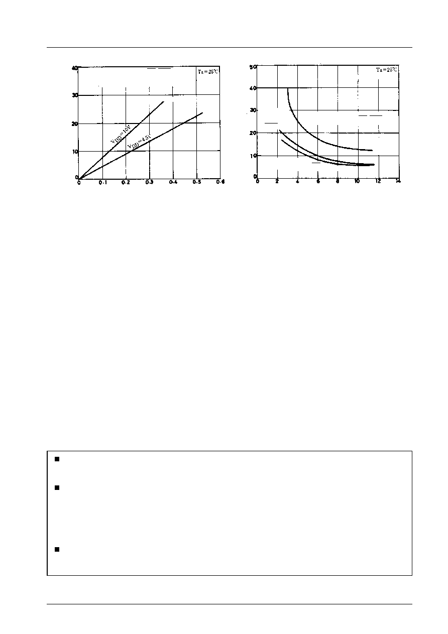
Segment outputs other than PM, 5b&e
This data is in case of flowing current to one
segment only.
Output
current,
I
OL
≠m
A
Output voltage, V
OL
≠ V
Output
impedance,
R
OUT
≠
Segment outputs
(I
OL
= 15 mA) other than PM, 5b&e
Segment
output
(I
OL
= 30 mA)
of 5b&e
Segment output
(I
OL
= 45 mA) of PM
Supply voltage , V
DD
≠ V
I
OL
≠ V
OL
R
OUT
≠ V
DD
LC7267
PS No. 1511- 10/10