 | –≠–ª–µ–∫—Ç—Ä–æ–Ω–Ω—ã–π –∫–æ–º–ø–æ–Ω–µ–Ω—Ç: LC72705 | –°–∫–∞—á–∞—Ç—å:  PDF PDF  ZIP ZIP |
Overview
The LC72705E is a data demodulation IC for receiving
FM multiplex broadcasts for mobile receivers in the
DARC format. This IC includes a decoder circuit that
performs the required VICS processing, and, in
conjunction with a bandpass filter IC (either the
LV3400M or the LV3403M), can form a compact yet
high-functionality VICS reception system. Note that a
contract with VICS Center is required to evaluate this IC
and to produce end products that support VICS.
Applications
∑ Receivers for DARC format mobile receiver FM
multiplex broadcasts
Functions
∑ MSK delay detection circuit based on a 1T delay
∑ Error correction function based on a 2T delay (in the
MSK detector stage)
∑ Digital PLL based Clock regeneration circuit
∑ Shift-register type 1T and 2T delay circuits
∑ Block and frame synchronization detection circuit
∑ Function for setting the number of allowable BIC errors,
the number of synchronization protection states
∑ Error correction using (272, 190) codes
∑ Layer 4 CRC code checking circuit
∑ On-chip frame memory and memory control circuit for
vertical correction
∑ 7.2-MHz crystal oscillator circuit
∑ VICS decoder circuit
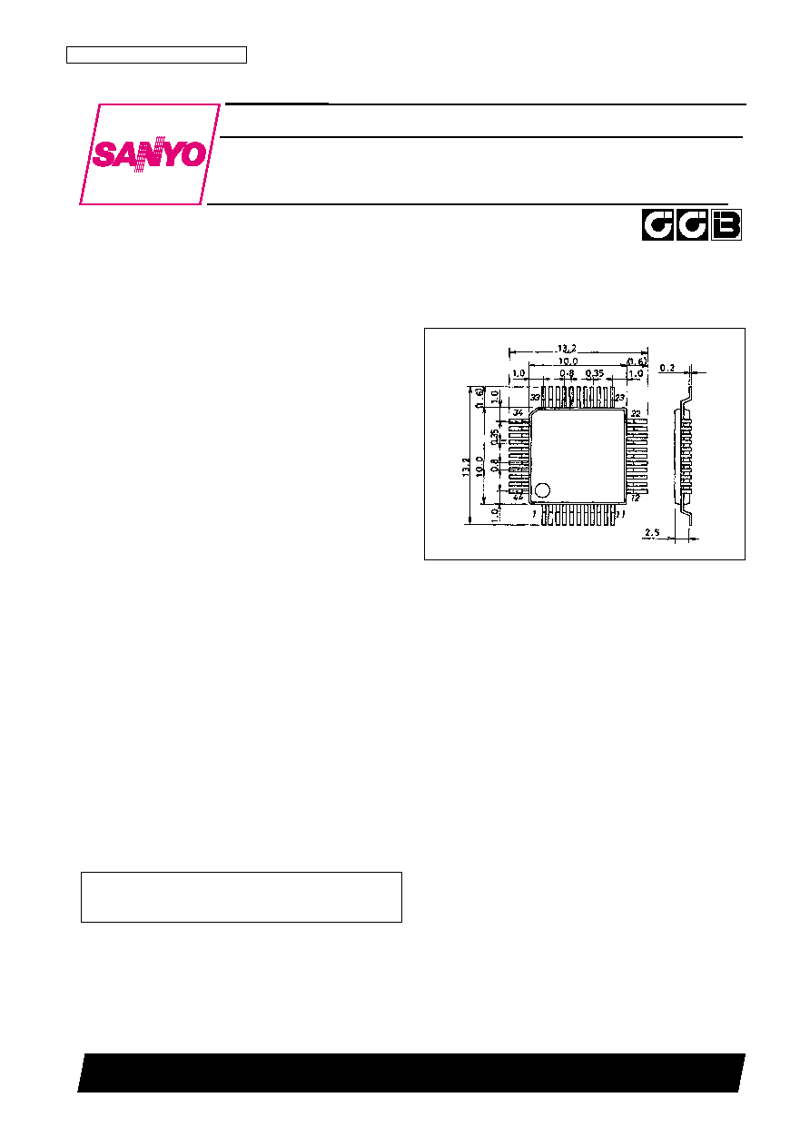
Package Dimensions
unit: mm
3148-QFP44MA
CMOS IC
51198RM (OT) No. 5744-1/14
SANYO: QFP44MA
[LC72705E]
SANYO Electric Co.,Ltd. Semiconductor Bussiness Headquarters
TOKYO OFFICE Tokyo Bldg., 1-10, 1 Chome, Ueno, Taito-ku, TOKYO, 110-8534 JAPAN
FM Multiplex Receiver IC for VICS Systems
LC72705E
Ordering number : EN5744
∑ CCB is a trademark of SANYO ELECTRIC CO., LTD.
∑ CCB is SANYO's original bus format and all the bus
addresses are controlled by SANYO.
No. 5744-2/14
LC72705E
Parameter
Symbol
Conditions
Ratings
Unit
Maximum supply voltage
V
DD
max
≠0.3 to +7.0
V
Input voltage
V
IN
1
CE, CL, DI, RST, STNBY
≠0.3 to +7.0
V
V
IN
2
Pins other than V
IN
1
≠0.3 to V
DD
+ 0.3
V
Output voltage
V
OUT
1
DO
≠0.3 to +7.0
V
V
OUT
2
Pins other than V
OUT
1
≠0.3 to V
DD
+ 0.3
V
Output current
I
OUT
BLOCK, FLOCK, DO
0 to 4.0
mA
Allowable power dissipation
Pd max
Ta
85∞C
400
mW
Operating temperature
Topr
≠40 to +85
∞C
Storage temperature
Tstg
≠55 to +125
∞C
Specifications
Absolute Maximum Ratings
at Ta = 25∞C, V
SS
= 0 V
Parameter
Symbol
Conditions
Ratings
Unit
min
typ
max
Supply voltage
V
DD
2.7
5.5
V
Input high-level voltage
V
IH
1
CL, CE, DI, RST, STNBY
0.7 V
DD
5.5
V
V
IH
2
MSK
0.7 V
DD
V
DD
V
Input low-level voltage
V
IL
1
Applies to the same pins as V
IH
1
V
SS
0.3 V
DD
V
V
IL
2
Applies to the same pins as V
IH
2
V
SS
0.3 V
DD
V
Oscillator frequency
F
OSC
This IC operates at frequencies within a
7.2
MHz
±250 ppm precision.
With a capacitance-coupled sine wave input
V
XI
to X
IN
400
1500
mVrms
Input sensitivity
V
DD
= +4.5 V to +5.5 V
With a capacitance-coupled sine wave input
V
XI
to X
IN
400
900
mVrms
V
DD
= +2.7 V to +3.6 V
[Serial I/O
*
]
Clock low-level time
t
CL
CL
0.7
µs
Clock high-level time
t
CH
CL
0.7
µs
Data setup time
t
SU
CL, DI
0.7
µs
Data hold time
t
HD
CL, DI
0.7
µs
CE wait time
t
EL
CL, CE
0.7
µs
CE setup time
t
ES
CL, CE
0.7
µs
CE hold time
t
EH
CL, CE
0.7
µs
Data latch change time
t
LC
CE
0.7
µs
Data output time
t
DDO
DO, CL
277
555
ns
Layer 4 CRC change time
t
CRC
CRC4, CL
0.7
µs
Allowable Operating Ranges
at Ta = ≠40 to +85∞C, V
SS
= 0 V
Parameter
Symbol
Conditions
Ratings
Unit
min
typ
max
V
OH
1
I
O
= 1 mA, FILCK
V
DD
≠ 1.0
V
Output high-level voltage
V
OH
2
I
O
= 2 mA, BLOCK, FLOCK,
V
DD
≠ 0.4
V
INT, CLK16, DATA
V
OL
1
I
O
= 1 mA, applies to the same pins as V
OH
1
1.0
V
Output low-level voltage
V
OL
2
I
O
= 2 mA, applies to the same pins as V
OH
2
0.4
V
V
OL
3
I
O
= 2 mA, DO
0.4
V
Input high-level current
I
IH
1
V
IN
= 5.5 V, CE, CL, DI, RST, STNBY
1.0
µA
I
IH
2
V
IN
= V
DD
, input pins other than I
IH
1
1.0
µA
V
IN
= V
SS
, MSK, CL, CE, DI, RST,
Input low-level current
I
IL
STNBY, TP0 to TP8, TPC1 to 2
≠1
µA
TOSEL1 to 2, TEST
Output off leakage current
I
OFF
V
O
= V
DD
, DO
5
µA
Hysteresis voltage
V
HIS
MSK, CL, CE, DI, RST, STNBY
0.1 V
DD
V
Internal feedback resistor
R
f
X
IN
, X
OUT
1.0
M
Current drain
I
DD
16
25
mA
Electrical Characteristics (1)
at V
DD
= +4.5 to +5.5 V, in the allowable operating ranges
Note
*
: See the serial data timing chart.
No. 5744-3/14
LC72705E
Parameter
Symbol
Conditions
Ratings
Unit
min
typ
max
V
OH
1
I
O
= 0.5 mA, FILCK
V
DD
≠ 1.0
V
Output high-level voltage
V
OH
2
I
O
= 1 mA, BLOCK, FLOCK,
V
DD
≠ 0.4
V
INT, CLK16, DATA
V
OL
1
I
O
= 0.5 mA, applies to the same pins as V
OH
1
1.0
V
Output low-level voltage
V
OL
2
I
O
= 1 mA, applies to the same pins as V
OH
2
0.4
V
V
OL
3
I
O
= 1 mA, DO
0.4
V
Input high-level current
I
IH
1
V
IN
= 5.5 V, CE, CL, DI, RST, STNBY
1.0
µA
I
IH
2
V
IN
= V
DD
, input pins other than I
IH
1
1.0
µA
V
IN
= V
SS
, MSK, CL, CE, DI, RST,
Input low-level current
I
IL
STNBY, TP0 to TP8, TPC1 to 2
≠1
µA
TOSEL1 to 2, TEST
Output off leakage current
I
OFF
V
O
= V
DD
, DO
1
µA
Hysteresis voltage
V
HIS
MSK, CL, CE, DI, RST, STNBY
0.1 V
DD
V
Internal feedback resistor
Rf
X
IN
, X
OUT
2.5
M
Current drain
I
DD
8
12
mA
Electrical Characteristics (2)
at V
DD
= +2.7 to +3.6 V, in the allowable operating ranges
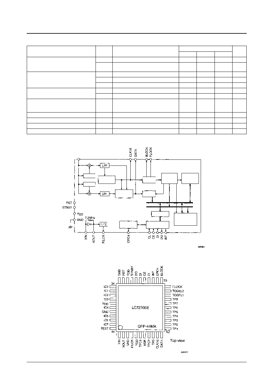
Block Diagram
Pin Assignment
MSK signal input
1T delay
2T delay
Clock
regeneration
MSK
correction
Layer 4 CRC
Output control
(CPU interface)
Synchronization
regeneration
Memory array
PN decoding
VICS processing
Timing
control
Error
correction
Layer 2 CRC
Data
Address
No. 5744-4/14
LC72705E
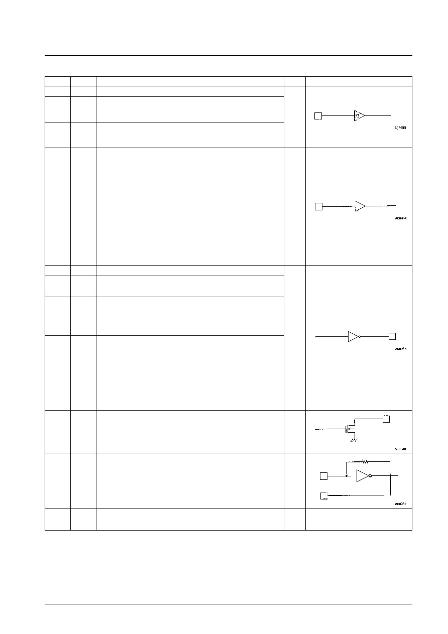
Pin Functions
Pin No.
Pin
Function
I/O
Circuit type
7
MSK
76-kHz MSK signal input (from the LV3400M/03M)
Input
Input
26
27
28
CL
CE
DI
CCB serial interface
Clock input
Data control input
Data input
32
30
44
RST
STNBY
TEST
System reset input (active low)
Standby mode (active high)
Test (Must be connected to ground during normal operation.)
9
12
13
14
15
16
17
18
19
6
8
20
21
TP0
TP1
TP2
TP3
TP4
TP5
TP6
TP7
TP8
TPC1
TPC2
TOSEL1
TOSEL2
Must be connected to either V
DD
or V
SS
.
Output
Output
4
FILCK
Reference clock output for the LV3400M/03M
10
11
CLK16
DATA
Clock regeneration monitor
Demodulated data monitor
23
22
24
25
BLOCK
FLOCK
CRC4
INT
Outputs a high level during block synchronization.
Outputs a high level during frame synchronization.
Layer 4 CRCC check result output
External CPU interrupt signal
34
35
36
37
39
41
42
43
IC0
IC1
IC2
IC3
IC4
IC5
IC6
IC7
Internal connections. These pins must be left open.
29
DO
Data output used by the CCB serial interface
Input
Output
1
2
XIN
XOUT
System clock generation crystal oscillator element connections
--
--
5, 31, 38
3, 33,40
V
DD
V
SS
Power supply (+2.7 to 5.5 V)
Ground
Data I/O Techniques
CCB Technique
Sanyo audio ICs input and output data using the Sanyo CCB (computer control bus) standard, which is a serial bus
format. This IC uses an 8-bit address CCB and uses the following addresses.
No. 5744-5/14
LC72705E
I/O mode
Address
Function
B0
B1
B2
B3
A0
A1
A2
A3
Input
0
1
0
1
1
1
1
1
16-bit control data input
Output
1
1
0
1
1
1
1
1
Data output for the input clock (CL)
Input
0
0
1
1
1
1
1
1
Data input (in 8-bit units) for the layer 4 CRC check circuit
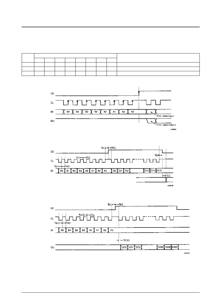
Data Input Timing
Note: The DO pin is normally left open.
Since the DO pin is an n-channel open drain pin, the time required for the data to change from the low level to the high level depends on the value of
the pull-up resistor.
Data Output Timing
I/O mode datermined
Internal data latching
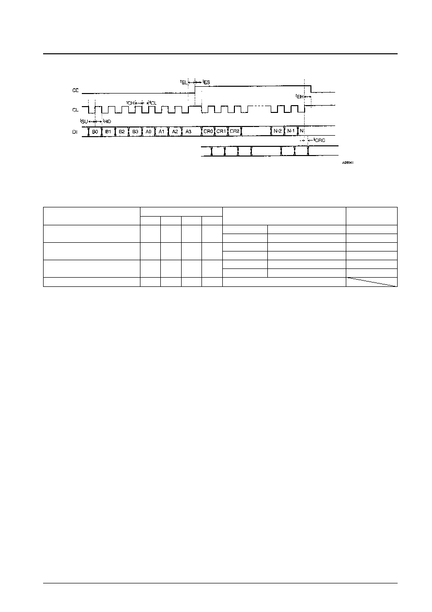
Layer 4 CRC Data Input Timing
Serial Control Data Input Settings
The input data consists of 16 bits (DI0 to DI15). The upper 8 bits (DI8 to DI15) are the control address and the lower 8
bits (DI0 to DI7) are the input data. Bits DI12 to DI15 are ignored.
∑ Number of allowed BIC errors
This IC's synchronization circuit operates by recognizing a 16-bit BIC code. The number of allowed errors is the
number of allowed error bits in the 16 bits used for BIC recognition. This data item allows the forward protection mode
(used when synchronized) and the backward protection mode (used when not synchronized) values to be set
independently. The default value is to allow up to 2 error bits in both the forward and backward directions. We
recommend setting the backward protection mode number of allowable BIC errors to 1 or 0 if the block
synchronization recognition output (the BLOCK pin, pin 23) is used to recognize the presence or absence of FM
multiplex data.
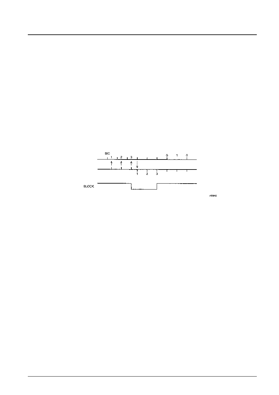
∑ Block synchronization errors protection count
The synchronization protection count can be set independently in the forward and backward directions. The protection
count conditions are as follows.
-- Backward protection (unsynchronized, BLOCK = low)
When the timing of the IC's internal synchronization free-running counter matches that of the received BIC, the
protection count is incremented by 1. Similarly, if the IC internal counter and the received BIC do not match, the
counter is cleared to 0. The count timing is the timing of the IC internal counter.
-- Forward protection (synchronized, BLOCK = high)
Operation is the opposite of the backward case, namely, the protection count is incremented when the timing of the
IC's internal synchronization free-running counter does not match that of the received BIC, and the protection
count is cleared to zero when the timing matches.
Figure 1 shows the protection counter when both the forward and backward protection counts are set to 3. This IC
defines the protection counter value to be 1 at the point where a match or a mismatch occurs between the IC
internal timing and the received BIC timing. For example, a backward protection count of 2 corresponds to the case
where the IC internal timing and the received BIC timing match two times consecutively. To set the protection data
to new values, applications must send data in which 1 has been subtracted from the desired values, e.g. to set up
protection counts of 3 as shown in figure 1, applications must send the value 22H. Similarly, if the value set is 00,
due to the definition, the protection counts for both the forward and backward directions will be set to 1. However,
from an operation standpoint, this corresponds to operation equivalent to there being no protection circuit. The
default values are a forward protection count of 8 and a backward protection count of 2. We recommend resetting
the block synchronization backward protection count to a value more strict than the default, e.g. to a value of 3 or
more as opposed to the default of 2, if the block synchronization recognition output (the BLOCK pin, pin 23) is
used to recognize the presence or absence of FM multiplex data.
No. 5744-6/14
LC72705E
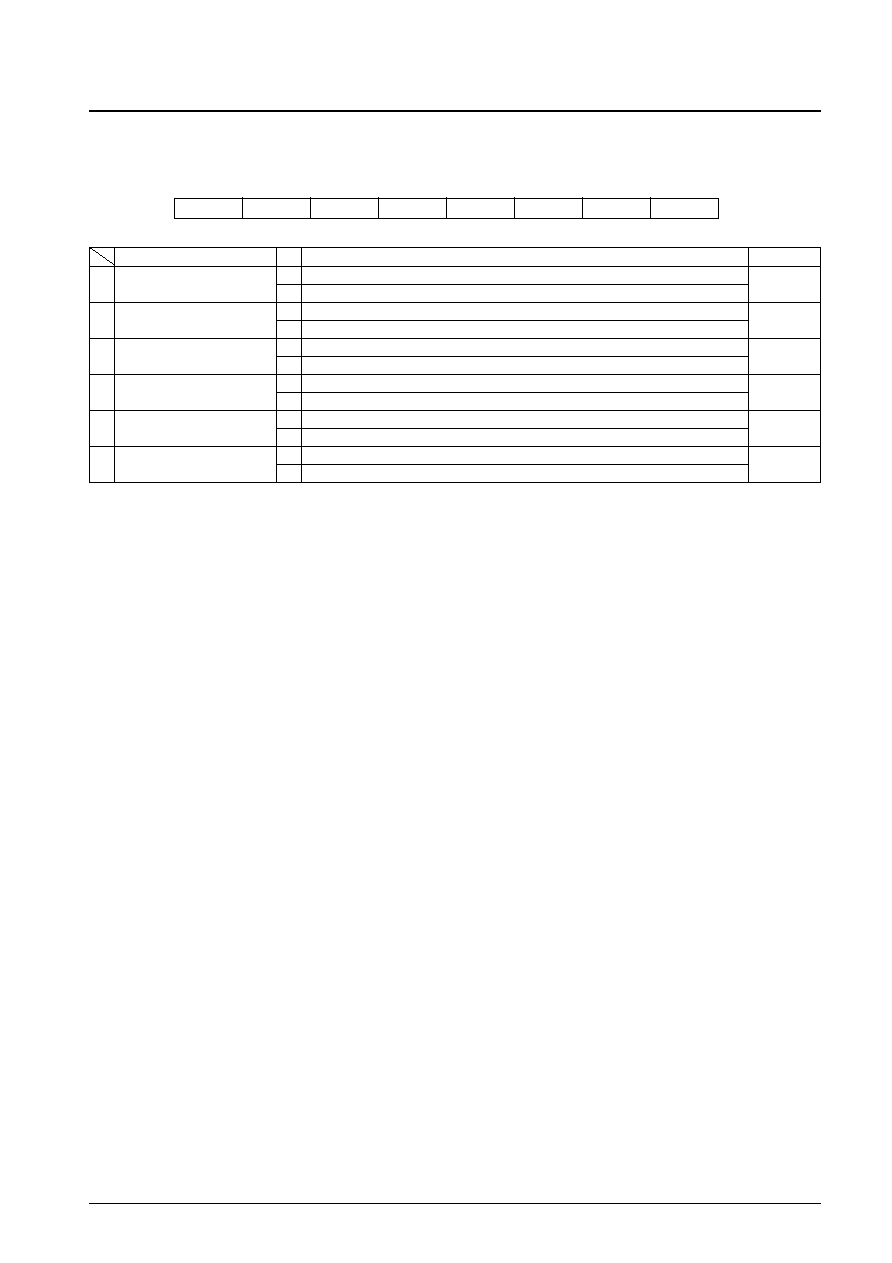
CRC4 pin output
Register
Address
Data
Default setting
DI11
DI10
DI9
DI8
Number of allowable BIC errors
0
0
0
0
Upper 4 bits
Allowed error bits backward
2
Lower 4 bits
Allowed error bits forward
2
Number of block error protection states
0
0
0
1
Upper 4 bits
Block backward protection
1
Lower 4 bits
Block forward protection
7
Number of frame error protection states
0
0
1
0
Upper 4 bits
Frame backward protection
1
Lower 4 bits
Frame forward protection
7
Control register
0
0
1
1
See the control register description on page 8
CRC4 output after N items transferred
Note: The N items are 8-bit units.
∑ Frame synchronization error protection count
This IC detects the four unique BIC inflection points that exist in a single frame, and increments or decrements the
protection counter depending on whether or not the IC internal frame synchronization counter matches. The data values
are set in the same way as those for the block synchronization protection count are set, namely data in which 1 has been
subtracted from the desired protection count must be transferred. The frame synchronization default values are 8 for
forward protection and 2 for backward protection.
∑ Control registers
These registers are used to set the IC operating mode. These are described later.
∑ Notes
-- The address bits DI12 to DI15 are ignored.
-- Addresses other than those listed above (for example location 0110) are special addresses used for test mode and
other special IC functions. Do not set these locations.
-- The default values are the values reloaded into the internal registers when a reset signal (RST) is received. These
values are the recommended values for normal operation, and normally do not need to be modified. If only the
default values are used, there is no need to provide data transfer routines in the external CPU or microcontroller.
Layer 4 CRC Check Circuit
This is a function provided for data group error detection, i.e. layer 4 CRC. After the stipulated number of bytes of data
group data and a 16-bit CRC error check word are transferred, the CRC4 pin outputs a high level if there were no errors.
The CRC4 pin outputs a high level if all the bits in the IC internal CRC check register were 0. When using this function
to perform the layer 4 CRC check, the IC internal CRC check register must be initialized before a single data group data
unit is transferred. This register is initialized by sending bit 7 of the control register. Note that since this flag is not
automatically reset to 0, the application must return it to 0 before transferring layer 4 CRC check data. If there were no
errors in any of the received data groups, the CRC register will always be all zeros after the CRC check of a single data
group. Therefore, the above control register initialization will not be necessary as long as there are no errors in the layer 4
CRC. The data length of the transferred data group data is in units of 8 bits. Also note that while there is no upper limit
on the amount of data transferred in a single operation, data transfers may also be divided into multiple transfer
operations.
No. 5744-7/14
LC72705E
Note:
*
Both forward and backward protection counts are 3.
Figure 1 Block Synchronization Protection Operation (forward
backward
forward)
Received data
Synchronization
counter BIC position
Reset
Control Register
Detailed Descriptions
∑ VEC HALT
Setting this flag stops all IC operations related to vertical and second horizontal correction. Data output is limited to
data following the first correction.
∑ EC STOP
This flag stops all operations (including RAM access) related to error correction and all data output operations. While
all IC operations are stopped in standby mode, MSK demodulation, the synchronization circuit, the serial data input
circuit, and the layer 4 CRC circuit continue to operate in this mode.
∑ SYNC RST
Clears the synchronization state and the synchronization protection state in the synchronization block and sets that
block to the unsynchronized state. This allows quick frame synchronization pull in when, during receiver tuning
operations, the frame period of the new reception data after station selection is displaced. While this flag is used for
initialization of synchronization related circuits, it does not initialize the number of allowed BIC errors, the block
synchronization forward and backward protection settings, and the frame synchronization forward and backward
protection settings. During the synchronization block reset, the INT signal is not output and the DO pin outputs a high
level (high impedance). Since this flag is not automatically reset to 0, applications must send data again to set it to 0.
∑ INT MOVE
The data output by this IC is fully corrected, and only data received during both block and frame synchronization is
output. (The level 2 CRC check is included.) This flag must be set to acquire all data in the same manner as the
LC72700E.
∑ DO MOVE
In the LC72700E, the DO pin output was linked to and changed with the INT signal so that it could be used in place of
the INT CPU interrupt signal. Set this flag to use that function.
No. 5744-8/14
LC72705E
Bit
Function
Initial value
2
VEC HALT
L
Vertical correction and second horizontal correction: enabled
L
(Vertical error correction stop)
H
Vertical correction and second horizontal correction: disabled
3
EC STOP
L
All functions operate
L
(Error correction stop)
H
Only the MSK detection and synchronization regeneration circuits operate
4
SYNC RST
L
L
(Synchronization block reset)
H
Only the synchronization circuit is reset
5
INT MOVE
L
Only the correction complete, layer 2 CRC complete, and data received while synchronized are output
L
(INT type)
H
All data is output. (Operation identical to that of the LC72700)
6
DO MOVE
L
The high-level (high-impedance) state is held at times other than data output
L
(DO pin operation)
H
The DO pin changes with the INT pin. (Operation identical to that of the LC72700)
7
CRC4 RST
L
L
(Layer 4 CRC)
H
The layer 4 CRC circuit is reset to its initial state
Control register
VEC HALT
EC STOP
SYNC RST
INT MOVE
DO MOVE
CRC4 RST
0
1
2
3
4
5
6
7
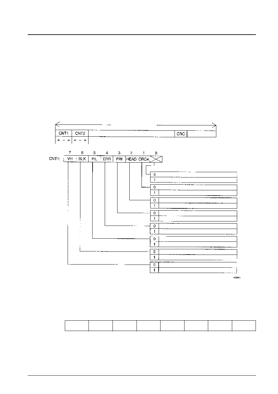
Structure of the Output Data
∑ The output data consists of a total of 288 bits (36 bytes). The first two bytes are status information, and data is output in
a single data block unit.
∑ CNT1 and CNT2 are output LSB first.
∑ The corrected data is output starting with the first bit in the data block.
∑ BIC codes are not output.
Note: The CPU can easily select data by discriminating the status information at first during data readout. Data that is
determined to be unnecessary can be immediately cancelled without reading it out. (The CPU can simply ignore
the data until the next interrupt arrives.)
For example, the CPU can also read out just the first 22 bytes (the data block section) of the corrected data, and
does not have to read out the unrequired 12 bytes (the layer 2 CRC and parity data).
No. 5744-9/14
LC72705E
Notes:
∑ CRC indicates the layer 2 CRC check when the ERR flag is 1.
∑ The CRC4 result is the data immediately preceding the point when the CCB output address (#FB) was input and CE was high.
∑ The HEAD flag is only valid for horizontal correction data output, i.e. when VH is 0.
BLNK0 to BLNK7: Indicates either the block number for the output data or the parity block number.
The data blocks in a single frame are numbered 0 to 189, and the parity blocks are numbered 0 to 81.
Parity block data is not output for post-horizontal correction output.
CNT2:
BLN7
BLN6
BLN5
BLN4
BLN3
BLN2
BLN1
BLN0
7
6
5
4
3
2
1
0
8 bits
8 bits
288 bits (36 bytes)
Corrected data
176 bits
Parity
Layer 4 CRC shift register: Not all zeros
Layer 4 CRC shift register: All zeros (no errors)
Normal block data
Data for the first block is being output
Parity block data
Error correction and CRC check OK
Either an uncorrectable error or the NG CRC check
Indicates data received with frame synchronization not achieved
Indicates data received with frame synchronization achieved
Indicates data received with block synchronization not achieved
Indicates data received with block synchronization achieved
Output with horizontal correction only
Output after vertical correction
*
Bit 0 is unused.
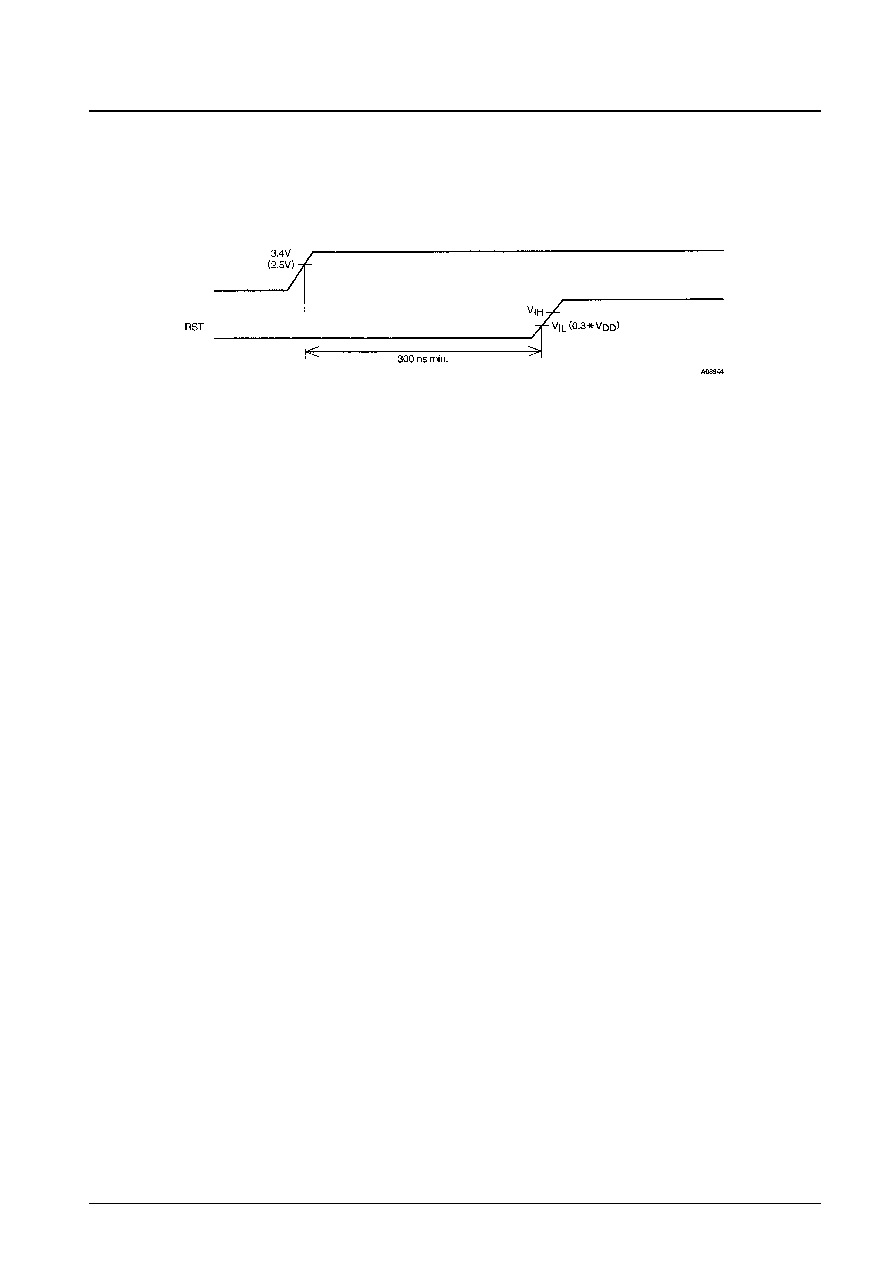
Operation During Reset and in Standby Mode
∑ The reset signal
A reset operation is performed by holding the RST pin input level under V
IL
for at least 300 ns when the power-supply
voltage (V
DD
) is over 3.4 V (or over 2.5 V when a 3-V V
DD
is used.) See the figure below. Applications must apply a
reset when power is first applied or when power is reapplied.
∑ Pin outputs during a reset
Low-level outputs: FILCK (4), CLK16 (10), DATA (11), FLOCK (22), BLOCK (23), CRC4 (24), IC0 (34) to IC3
(37), IC4 (39), IC5 (41), IC6 (42)
High-level outputs: INT (25), XOUT (2)
Open:
DO (29)
∑ Reset operating range
The output pin states according to the reset signal are stipulated by item "Pin outputs during a reset" above. The IC
internal flip-flops are all reset. Although the delay shift registers are also reset, the memory array is not influenced.
However, since memory refresh operation stops, data cannot be retained. The crystal oscillator circuit does not stop.
∑ Data input after a reset
After a reset completes and at least one full clock cycle (about 278 ns at 3.6 MHz, this is the IC's main clock) has
elapsed, the serial input control circuit will be able to operate and accept data.
∑ Standby mode
The IC can be set to standby mode by setting the STNBY pin high. Since all IC operations are stopped in this mode,
this produces a state essentially equivalent to the power off state. (Note that after standby mode has been cleared, a wait
period is required until the crystal oscillator circuit is operating stably.) The pin output states in standby mode are
identical to the states after a reset as described in item "Pin outputs during a reset" above.
Notes on Post Error Correction Output Data
∑ The received data is error corrected using (272, 190) codes in single block (272 bits) unit. An error check using the
layer 2 CRC is also performed. After error correction, the IC prepares for transfer of the data to the CPU and outputs
the INT signal. This is referred to as horizontal correction output.
∑ However, the INT signal is not output at this time if the corresponding output data does not meet all of the following
three conditions.
-- Error correction completed and it passed the layer 2 CRC check.
-- The data was received while both block and frame synchronization were established.
-- The data was packet data.
Note that all received packet data can be acquired by setting bit 5 (INT) in the control register.
∑ If the data could not be corrected by the horizontal correction system, correction using product codes is performed in
frame units. This is called vertical correction. The data that can be acquired at the output of the vertical correction is the
following.
-- Data that was fully corrected in horizontal correction is not output.
-- Packet data that could not be corrected by horizontal correction but that was fully corrected by vertical correction is
output.
-- Packet data that could not be corrected by either horizontal or vertical correction is not output.
Note that, as is the case for horizontal correction output, all received packet data can be acquired by setting bit 5 (INT)
in the control register. However, the parity packet data corrected by vertical correction cannot be output even if this
flag bit is set.
No. 5744-10/14
LC72705E
V
DD
voltage
∑ To prevent unnecessary error correction, the vertical correction is not applied to packets that were fully corrected by
horizontal correction or to packets that had no errors.
∑ Vertical correction is executed when all packet data in the object data was received while frame synchronization was
established and not all of the packet (block) data was corrected by horizontal correction. Vertical correction is not
performed if a whole frame of data with no errors is received, or if the frame was not synchronized. Also, the
corresponding post-vertical correction output data is not output.
∑ All data can be output, regardless of the correction complete/incomplete, synchronized/unsynchronized reception,
data/packet status or other conditions by setting bit 5 (INT) in the control register to 1.
CPU Interface Basic Restrictions
To save internal memory, this IC uses the smallest possible output buffer. Since the data that the IC receives is written to
memory without any breaks, if data readout is delayed post-correction data that should be read out will be overwritten by
the next data to be output. The output timings in this IC for post-correction (horizontal and vertical) data are stipulated as
follows.
∑ When preparation of the output data has completed, the IC issues a transfer request by setting the INT pin low.
∑ For data output, there are periods in which only horizontal data can be output and periods in which both time-sharing
horizontal data and vertical data can be output.
∑ Data transfers must be completed within about 9 ms after the INT pin goes low. For periods in which only post-
horizontal correction data can be output, data can be transferred over a period of about 18 ms. Even if the CPU is in the
midst of a read operation, the next output data will be written to the output buffer after the specified period elapses.
∑ Only one block of data can be read for a single transfer request (INT) for both vertical and horizontal correction. After
vertical correction processing completes, the post-vertical correction data is output in order starting with block number
1, and the parity block data is not output.
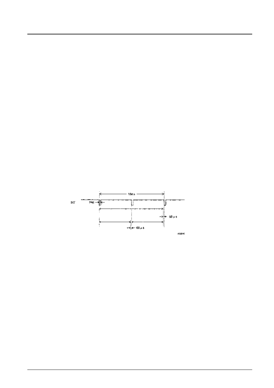
Notes on Data Output Timing (The relationship with the received data)
Figure 3 shows the timing relationship between the received data and the interrupt control signal INT. However, the
delay component relative to the actually received signal due to the demodulation operations in the MSK demodulation
block is ignored. Block synchronization is established by recognizing the BIC code. As shown in figure 3, the data for the
nth packet can be output during the reception of the next packet, packet number n + 1.
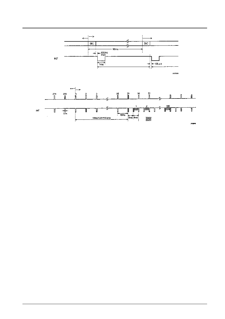
Figure 4 shows the output timing for vertical correction data. Vertical correction is used when the data for a whole frame
is stored in memory, frame synchronization is established, and furthermore horizontal correction was not able to correct
all the packet data. The timing for the start of vertical correction execution is the head of the frame. During reception of
packets 1 to 28 in the nth frame, horizontal correction is performed on each packet, data is passed to the CPU, and the
remaining unused processing time during that interval is used to apply vertical correction to the data from the previous
frame (frame n - 1). The post-vertical correction data (190 blocks of data) is output in order starting when the 29th packet
(block) is received at the rate of one block of output data for every block received. Of the data in the FM multiplex
broadcast frame structure, only the data in the data blocks is output, and the 190th block (the last data block) is output
while the 218th block is being received. As discussed previously (page 10), of the post-vertical correction output data, the
packet data for which horizontal correction completed fully is not output (the INT signal is not issued). However, it is not
the case that the vertical output is speeded up by the amount of the packet data that is not output. For example, if data
packets 1 to 100 were fully corrected in horizontal correction, the point that the 101st post-vertical correction packet data
is output will not be the reception position block number 29 in figure 4, but the reception position of packet data number
129.
No. 5744-11/14
LC72705E
Figure 2 Basic Interface Timing
Only horizontal data output
Horizontal and vertical data output
Horizontal data output
period
Period when
data cannot be
guaranteed
Vertical data output period
Horizontal data output
period
Notes on Output Data Selection During Tuning (Provided for reference purposes)
A tuning system is required in an FM multiplex broadcast reception system. However, applications must perform the
following processing if it is unacceptable for the IC to output data for the previous station after tuning a new station.
∑ Set bit 4 (SYNC RST) in the control register during tuning to set the synchronization circuit to the unsynchronized state.
∑ If bit 5 (INT) in the control register is enabled, do not use the post-vertical correction output (data for which bit 7 in the
status flag CNT1 is 1) until frame synchronization is re-established.
Of the DARC FM multiplex processing, this IC performs the processing through error correction (layer 2) without
requiring any special control operations. The IC itself is not able to recognize whether the content of the received data
has changed or whether the system has been tuned to another station. Therefore the application system must use the
above procedure to command the IC not to output the old data and only to output the new data. The synchronization
relationship between the stations is also problematic; although it is rare that the frames of the previous station and the
next station would be synchronized, applications must also perform the processing described above to cancel the frame
synchronization forward protection period.
Differences in Data Output between this IC and the LC72700E (Provided for reference purposes)
The LC72700E provided all data that could be provided to the microcontroller in the later stages of the system, and was
designed so that the microcontroller was required to decide whether to accept or discard the data by checking the status
output. For example, a received data packet could be output as post-horizontal correction data and then again, a few
seconds later, could be output as post-vertical correction data. Data with no errors, or data that could be corrected by
horizontal correction was output twice as identical data. This IC implements the conditions shown on page 10
(in "Notes on Post Error Correction Output Data") concerning data with no errors. Stated simply, this IC does not output
data unnecessarily. For example, the INT signal will not be output for data from a received station that is not
broadcasting multiplexed data. Also, under good reception conditions where there are no errors, there will be no post-
vertical correction output and the INT signal period will be 18 ms.
There are cases where it may become impossible to acquire the data if the microcontroller software includes the data
acquisition conditions required for the LC72700E. For example, this problem may occur if the software was designed to
only use the post-vertical correction output. Since this IC does not output the same data twice and does not output bad
data at all, applications do not need to select from the input data if they simply acquire all data that starts at every INT
signal. (In other words, it can be also said that this IC does not generate any unnecessary interrupt signals.) To set up this
IC to provide the same output format as that of the LC72700E, applications must set bit 5 (INT MODE) in the control
register to 1. Note that this IC is added a control function that causes the IC not to output post-vertical correction data if
the vertical correction operation was not executed. Since this control function is not influenced by the INT MOVE flag,
post-vertical correction output is not provided during error-free reception even if the INT MOVE flag was set. Thus care
is required in application software design.
No. 5744-12/14
LC72705E
Figure 3 Timing of Data Reception and Block Synchronization Data Output
Figure 4 Vertical Correction Data Output Timing
Reception data
Packet (N ≠ 1)
Packet data N
Packet (N + 1)
Output period for packet data (N ≠ 1)
Period that data cannot be
guaranteed
Output of packet data N
Frame N ≠ 1
Frame N
Reception
block number
BIC period
Output period for the post-vertical correction
data from the previous frame
No. 5744-13/14
LC72705E
*Announcement*
Sanyo Electric Co., Ltd. reports to NHK-ES data for the
number of units of this IC shipped after October 1997.
(However, this does not apply to samples.)
*Address inquiries concerning contracts to:
NHK Engineering Services
Telephone: +81-3-3417-4840
The DARC (Data Radio Channel) FM multiplex broadcast
technology was developed by NHK (Japan Broadcasting
Corporation). DARC is a registered trademark of NHK
Engineering Service (NHK-ES).
A separate contract with NHK-ES is required in advance
for the manufacture and/or sale of electronic equipment
that uses DARC technology. Note that the logo shown
here can be displayed on electronic equipment that uses
DARC technology.
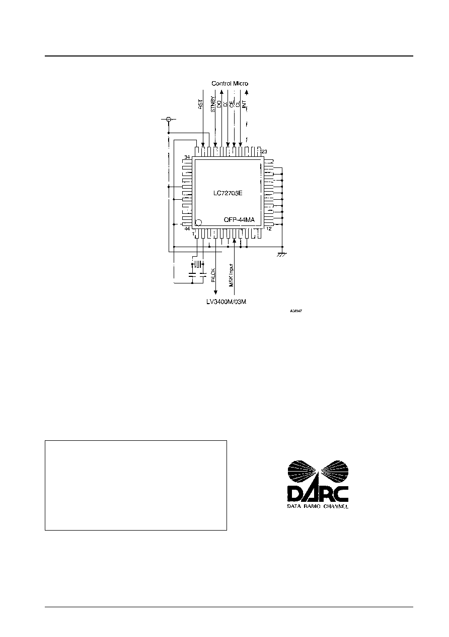
Connection Example (Provided for reference purposes.)

PS No. 5744-14/14
LC72705E
This catalog provides information as of May, 1998. Specifications and information herein are subject to change
without notice.
s
No products described or contained herein are intended for use in surgical implants, life-support systems, aerospace
equipment, nuclear power control systems, vehicles, disaster/crime-prevention equipment and the like, the failure of
which may directly or indirectly cause injury, death or property loss.
s
Anyone purchasing any products described or contained herein for an above-mentioned use shall:
Accept full responsibility and indemnify and defend SANYO ELECTRIC CO., LTD., its affiliates, subsidiaries and
distributors and all their officers and employees, jointly and severally, against any and all claims and litigation and all
damages, cost and expenses associated with such use:
Not impose any responsibility for any fault or negligence which may be cited in any such claim or litigation on
SANYO ELECTRIC CO., LTD., its affiliates, subsidiaries and distributors or any of their officers and employees
jointly or severally.
s
Information (including circuit diagrams and circuit parameters) herein is for example only; it is not guaranteed for
volume production. SANYO believes information herein is accurate and reliable, but no guarantees are made or implied
regarding its use or any infringements of intellectual property rights or other rights of third parties.