 | –≠–ª–µ–∫—Ç—Ä–æ–Ω–Ω—ã–π –∫–æ–º–ø–æ–Ω–µ–Ω—Ç: LC72714 | –°–∫–∞—á–∞—Ç—å:  PDF PDF  ZIP ZIP |
Ordering number : ENN6871A
92001TN (OT) No. 6871-1/29
Overview
The LC72714W is data demodulator ICs for receiving FM
multiplex broadcasts for mobile reception in the DARC
format. This IC includes an on-chip bandpass filter for
extracting the DARC signal from the FM baseband signal.
It also integrates a decoder circuit that performs the VICS
data processing on the same chip and can implement a
compact, multifunction VICS reception system. The
LC72714W is an improved version of the LC72710W that
features circuit improvements that allow a single tuner to
receive both the VICS data and the dGPS data supported
by the earlier device. Note that a contract with VICS
Center is required to evaluate this sample IC and to
produce end products that support VICS.
Functions
∑ Adjustment-free 76 kHz SCF bandpass filter
∑ Built-in VICS decoder
∑ MSK delay detection system based on a 1T delay.
∑ Error correction function based on a 2T delay (in the
MSK detection stage)
∑ Digital PLL based clock regeneration function
∑ Shift-register 1T and 2T delay circuits
∑ Block and frame synchronization detection circuits
∑ Functions for setting the number of allowable BIC errors
and the number of synchronization protection
operations.
∑ Error correction using (272, 190) codes
∑ Built-in layer 4 CRC code checking circuit
∑ On-chip frame memory and memory control circuit for
vertical correction
∑ 7.2 MHz crystal oscillator circuit
∑ Two power saving modes: STNBY and EC STOP
∑ Dedicated frame synchronization circuit for
simultaneous reception of dGPS and VICS data
∑ Applications can use either a parallel CPU interface
(DMA) or a CCB serial interface.
∑ Supply voltage: 2.7 to 3.6 V
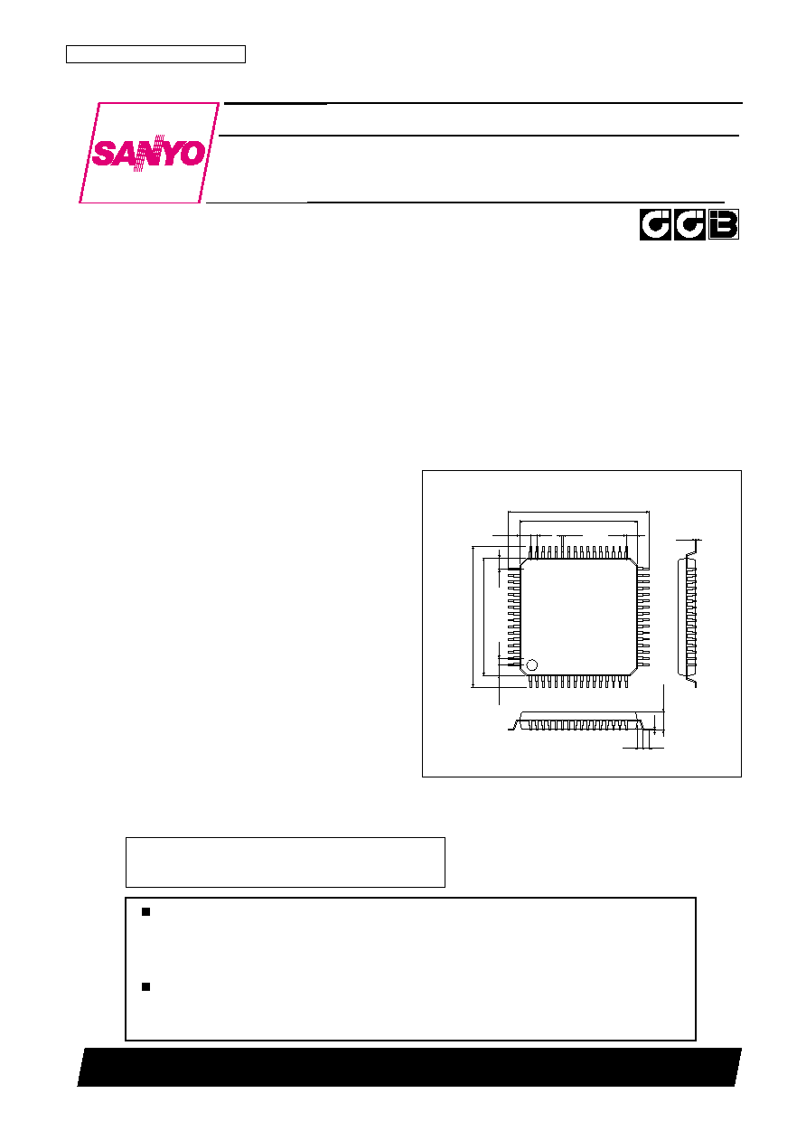
Package Dimensions
unit: mm
3190-SQFP64
10.0
12.0
1.25
0.5
1.25
1.25
0.5
1.25
0.18
12.0
1
16
17
32
33
48
49
64
10.0
0.5
1.7max
0.5
0.1
0.15
SANYO: SQFP64
[LC72714W]
LC72714W
SANYO Electric Co.,Ltd. Semiconductor Company
TOKYO OFFICE Tokyo Bldg., 1-10, 1 Chome, Ueno, Taito-ku, TOKYO, 110-8534 JAPAN
Mobile FM Multiplex Broadcast IC
with On-Chip VICS Decoder
CMOS IC
Any and all SANYO products described or contained herein do not have specifications that can handle
applications that require extremely high levels of reliability, such as life-support systems, aircraft's
control systems, or other applications whose failure can be reasonably expected to result in serious
physical and/or material damage. Consult with your SANYO representative nearest you before using
any SANYO products described or contained herein in such applications.
SANYO assumes no responsibility for equipment failures that result from using products at values that
exceed, even momentarily, rated values (such as maximum ratings, operating condition ranges, or other
parameters) listed in products specifications of any and all SANYO products described or contained
herein.
∑ CCB is a trademark of SANYO ELECTRIC CO., LTD.
∑ CCB is SANYO's original bus format and all the bus
addresses are controlled by SANYO.
No. 6871-2/29
LC72714W
Parameter
Symbol
Conditions
Ratings
Unit
Maximum supply voltage
V
DD
≠0.3 to +5.5
V
Input voltage
V
IN
(1)
A0/CL, A1/CE, A2/DI, RST, STNBY
≠0.3 to +7.0
V
V
IN
(2)
Pins other than V
IN
(1)
≠0.3 to V
DD
+ 0.3
V
Output voltage
V
OUT
(1)
DO
≠0.3 to +7.0
V
V
OUT
(2)
Pins other than V
OUT
(1)
≠0.3 to V
DD
+ 0.3
V
Output current
I
OUT
(1)
INT, RDY, DREQ, and D0 to D15
0 to 4.0
mA
I
OUT
(2)
Pins other than I
OUT
(1)
0 to 2.0
mA
Allowable output current (total)
I
TTL
Total for all the output pins
20
mA
Allowable power dissipation
Pdmax
Ta
85∞C
200
mW
Operating temperature
Topr
≠40 to +85
∞C
Storage temperature
Tstg
≠55 to +125
∞C
Specifications
Absolute Maximum Ratings
at Ta = 25∞C, V
SS
= 0 V
Parameter
Symbol
Conditions
Ratings
Unit
min
typ
max
Supply voltage
V
DD
2.7
3.6
V
High-level input voltage
V
IH
1
A0/CL, A1/CE, A2/DI, RST, STNBY
0.7 V
DD
5.5
V
V
IH
2
DACK, WR, RD, CS, SP, BUSWD, A3, IOCNT1, IOCNT2
0.7 V
DD
V
DD
V
Low-level input voltage
V
IL
1
Pins for which V
IH
1 applies
V
SS
0.3 V
DD
V
V
IL
2
Pins for which V
IH
2 applies
V
SS
0.3 V
DD
V
Oscillator frequency
FOSC
This IC operates with a frequency precision of ±250 ppm
7.2
MHz
X
IN
input sensitivity
VXI
With a sine wave input to X
IN
, capacitor coupling,
400
900
mVrms
V
DD
= +2.7 to +3.6 V
VMPX
With a 100% modulated composite signal input to
120
500
mVrms
Input amplitude
MP
XIN
, V
DD
= +3.3 V
VMPX2
With a 100% modulated composite signal input to
120
450
mVrms
MP
XIN
, V
DD
= +2.7 V
Clock low-level period
t
CL
A0/CL
0.7
µs
Clock high-level period
t
CH
A0/CL
0.7
µs
Data setup time
t
SU
A0/CL, A2/DI
0.7
µs
Data hold time
t
HD
A0/CL, A2/DI
0.7
µs
CE wait time
t
EL
A0/CL, A1/CE
0.7
µs
CE setup time
t
ES
A0/CL, A1/CE
0.7
µs
CE hold time
t
EH
A0/CL, A1/CE
0.7
µs
Data latch change time
t
LC
A1/CE
0.7
µs
Data output time
t
DDO
DO, A0/CL
277
555
ns
CRC4 change time
t
CRC
CRC4, A0/CL
0.7
µs
Allowable Operating Ranges
at Ta = ≠40 to +85∞C, V
SS
= 0 V
Serial I/O
No. 6871-3/29
LC72714W
Allowable Operating Ranges: Parallel Interface
at Ta = ≠40 to +85∞C, V
SS
= 0 V
Notes:
Application designs must take the RDY signal output delay into consideration if the RDY signal is used as the CPU bus wait signal.
When the RDY signal is used, the "RD low-level width" and the "Corrected output RD width" values express the basic timing (excluding the wait
time) settings for the CPU bus.
If the RDY signal is not used, (that is, if no wait states are inserted) the value of the RD low-level width will be 280 ns (minimum).
Parameter
Symbol
Conditions
Ratings
Unit
min
typ
max
Address to RD setup
t
SARD
A0/CL, A1/CE, A2/DI, A3, RD
20
ns
RD to address hold
t
HARD
A0/CL, A1/CE, A2/DI, A3, RD, t
WRDL
=>250 ns
≠20
ns
RD low-level width
t
WRDL
1
RD
280
ns
RD low-level width (when RDY is used)
t
WRDL
2
RD
100
280
ns
RD cycle wait
t
CYRD
A0/CL, A1/CE, A2/DI, A3, RD
150
ns
RDY width (Register read)
t
WRDY
RDY
60
230
ns
RD data hold
t
RDH
RD, DATn
0
ns
Address to WR setup
t
SAWR
A0/CL, A1/CE, A2/DI, A3, WR
20
ns
WR to address hold
t
HAWR
A0/CL, A1/CE, A2/DI, A3, WR
20
ns
WR cycle wait
t
CYWR
A0/CL, A1/CE, A2/DI, A3, WR
150
ns
WR low-level width
t
WWRL
WR
200
ns
WR data hold
t
WDH
WR, DATn
0
ns
RDY output delay
t
DRDY
RD, RDY
0
50
ns
Corrected output RD width
t
WDRD
1
RD (BUSWD = L 8 bits)
300
ns
RD (BUSWD = H 16 bits)
540
ns
Corrected output RD width
t
WDRD
2
RD (BUSWD = L 8 bits)
100
300
ns
(when RDY is used)
RD (BUSWD = H 16 bits)
300
540
ns
RDY width (corrected output read)
t
WDRDY
RDY (BUSWD = L 8 bits)
60
230
ns
RDY ((BUSWD = H 16 bits)
300
490
ns
DACK to DREQ delay
t
DREQ
DREQ, DACK
260
ns
DMA cycle wait
t
CYDM
RD, DREQ
420
ns
RD low-level width (DMA)
t
WRDM
RD
300
ns
Parallel I/O
Electrical Characteristics
at V
DD
= +2.7 to +3.6 V, within the allowable operating ranges
Parameter
Symbol
Conditions
Ratings
Unit
min
typ
max
V
OH
1
Io = 1 mA, BCK, FCK, BLOCK, FLOCK,
V
DD
≠ 0.4
V
High-level output voltage
CRC4, CLK16DATA
V
OH
2
Io = 2 mA, INT, RDY, DREQ, D0 to D15
V
DD
≠ 0.4
V
V
OL
1
Io = 1 mA, Pins for which V
OH
1 applies
0.4
V
Low-level output voltage
V
OL
2
Io = 2 mA, Pins for which V
OH
2 applies
0.4
V
V
OL
3
Io = 1 mA, DO, INT
0.4
V
I
IH
1
V
IN
= 5.5 V, A0/CL, A1/CE, A2/DI, RST,
1.0
µA
High-level input current
STNBY
I
IH
2
V
IN
= V
DDD
, All input pins other than I
IH
1
1.0
µA
Low-level input current
I
IL
V
IN
= V
SSD
, All input pins
≠1.0
µA
Input resistance
Rmpx
MP
XIN
≠ Vssa f = 100 kHz
50
k
Reference supply voltage output
Vref
Vref, Vdda = 3 V
1.5
V
Bandpass filter center frequency
Fc
FLOUT
76.0
kHz
≠3 dB bandwidth
Fbw
FLOUT
19.0
kHz
Group delay
Dgd
FLOUT
≠7.5
+7.5
µs
Gain
Gain
FLOUT ≠ MPXIN f = 76 kHz
20
dB
ATT1
FLOUT f = 50 kHz
25
dB
Stop band attenuation
ATT2
FLOUT f = 100 kHz
15
dB
ATT3
FLOUT f = 30 kHz
50
dB
ATT4
FLOUT f = 150 kHz
50
dB
Output off leakage current
IOFF
V0 = V
DDD
, DO
1.0
µA
Hysteresis voltage
VHIS
A0/CL, A1/CE, A2/DI, A3, CS, RD, WR,
0.1 V
DDD
V
DACK, IOCNT1, IOCNT2, RST, STNBY
Internal feedback resistor
Rf
XIN, XOUT
1.0
M
Current drain
I
DD
12
20
mA
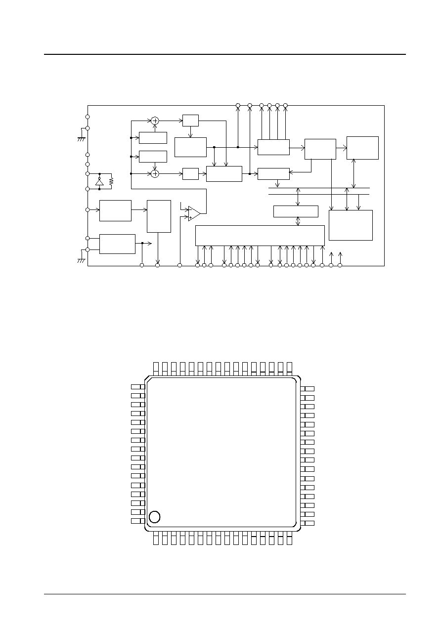
Block Diagram
No. 6871-4/29
LC72714W
VICS processing
PN decoding
Memory array
LPF
MPXIN
7.2MHz
Vref
XIN
Vssa
Vdda
XOUT
RST
CLK16
DATA
BCK
FCK
FLOCK
BLOCK
Data
Address
STNBY
Vssd
Vddd
LPF
Error correction:
layer 2 CRC
76kHz
BPF
(SCF)
Anti-aliasing
filter
Timing
control
Vref
Synchronization
regeneration
MSK correction
circuit
Clock
regeneration
2T delay
1T delay
IOCNT1
DACK
DREQ
IOCNT2
CRC4
FLOUT
CIN
VREF
CS
RD
WR
RDY
INT
BUSWD
TIN
SP
A3
DO
A2/DI
A1/CE
A0/CL
D0 to D15
Output control (CPU interface) and
layer 4 CRC detection circuit
Pin Assignment
IOCNT1
WR
RD
A0/CL
A1/CE
A2/DI
A3
CS
STNBY
BUSWD
SP
RST
32
D15
49
D14
D13
TIN
LC72714W
Vssa
D12
Vref
MPXIN
D11
D10
Vdda
D9
FLOUT
D8
NC
NC
CIN
D7
D6
TPC1
(Top view)
64
1
16
D5
TPC2
BCK
CRC4
FCK
BLOCK
FLOCK
DATA
CLK16
IOCNT2
Vddd
XOUT
INT
Vddd
Vssd
DO
NC
TEST
TOSEL1
TOSEL2
Vssd
XIN
Vddd
RDY
Vssd
DACK
DREQ
D4
D3
D2
D1
D0
No. 6871-5/29
LC72714W
Pin Functions
Pin No.
Pin
Function
I/O
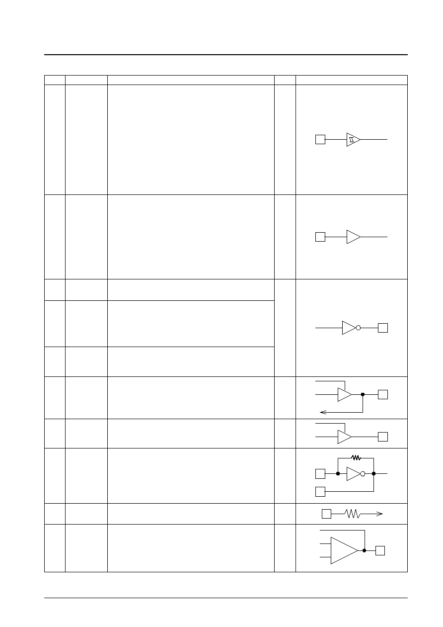
Pin circuit
Data bus I/O control 1 (SP = low)
*
1
Data bus I/O control 2 (SP = low)
*
1
DMA acknowledge (SP = low)
*
1
Write control signal (SP = low)
*
1
Read control signal (SP = low)
*
1
Address input 0 (SP = low) CCB CL input (SP = low)
1 (SP = low) CCB CE input (SP = low)
2 (SP = low) CCB DI input (SP = low)
3 (SP = low)
*
1
Chip select input (SP = L)
*
1
System reset input (negative logic)
Standby mode (positive logic)
3
4
13
38
39
40
41
42
43
44
46
45
IOCNT1
IOCNT2
DACK
WR
RD
A0/CL
A1/CE
A2/DI
A3
CS
RST
STNBY
SP = low: parallel, SP = high: serial
BUSWD = low: 8 bits, BUSWD = high: 16 bits
The test pin must be connected to the digital system ground (V
SS
).
Must be connected to the digital system power supply (V
DD
) or ground
(V
SS
) in normal operation.
As above
As above
As above
As above
47
48
60
58
59
61
62
49
SP
BUSWD
TEST
TPC1
TPC2
TOSEL1
TOSEL2
TIN
Clock regeneration monitor
Demodulated data monitor
5
6
CLK16
DATA
Frame start signal output
Block start signal output
Outputs a high level during frame synchronization
Outputs a high level during block synchronization
Level 4 CRC detection result output
9
10
7
8
11
FCK
BCK
FLOCK
BLOCK
CRC4
External CPU interrupt request output
DMA request signal
Read ready signal
Input
Input
Output
I/O
33
12
16
INT
DREQ
RDY
Data bus
The bus width can be set to be either 8 bits or 16 bits by the BUSWD
pin (pin 48).
For data input, only the lower 8 bits (D0 to D7) are valid.
*
3
17 to 24
D0 to D7
Output
Data bus (in 16-bit mode)
These pins are held in the output off state when BUSWD is low.
25 to 32
D8 to D15
I/O
Connections for the system clock crystal oscillator circuit.
The XIN pin can also be used as an external clock signal input.
64
1
XIN
XOUT
Input
Baseband (multiplex) signal input
53
MPXIN
≠
+
Output
Subcarrier output (76 kHz bandpass filter output)
55
FLOUT
Continued on next page.