
Overview
The LC72P366 is a single-chip PLL-plus-controller one-
time programmable PROM microcontroller that
corresponds to the Sanyo LC72358N, LC72362N, and
LC72366. The LC72P366 has the same package and pin
assignment as the LC72358N, LC72362N, and LC72366
mask ROM versions, and provides 32 KB of on-chip
PROM, organized as 16k words by 16 bits. The
LC72P366 can prove useful in reducing the startup times
for initial production runs and for reducing the switchover
time when end-product specifications change.
Features
∑ 32 KB (16k words
◊
16 bits) of on-chip PROM
-- This is a one-time programmable 32 KB (16k-word
◊
16-bit) PROM.
∑ Pin compatible with the mask ROM versions, i.e.
identical package and pin assignment.
Writing Sanyo ROMs
Sanyo provides a for-fee ROM writing service that
consists of writing data to the PROM in one-time
programmable PROM microcontrollers, printing,
screening, and data readout verification. Contact your
Sanyo sales representative for details.
Package Dimensions
unit: mm
3174-QFP80E
CMOS LSI
Ordering number :EN5544
N3096HA (OT) No. 5544-1/14
SANYO: QIP80E
[LC72P366]
SANYO Electric Co.,Ltd. Semiconductor Bussiness Headquarters
TOKYO OFFICE Tokyo Bldg., 1-10, 1 Chome, Ueno, Taito-ku, TOKYO, 110 JAPAN
On-Chip One-Time Programmable PROM
Single-Chip PLL Controller
LC72P366
∑ CCB is a trademark of SANYO ELECTRIC CO., LTD.
∑ CCB is SANYO's original bus format and all the bus
addresses are controlled by SANYO.
No. 5544-4/14
LC72P366
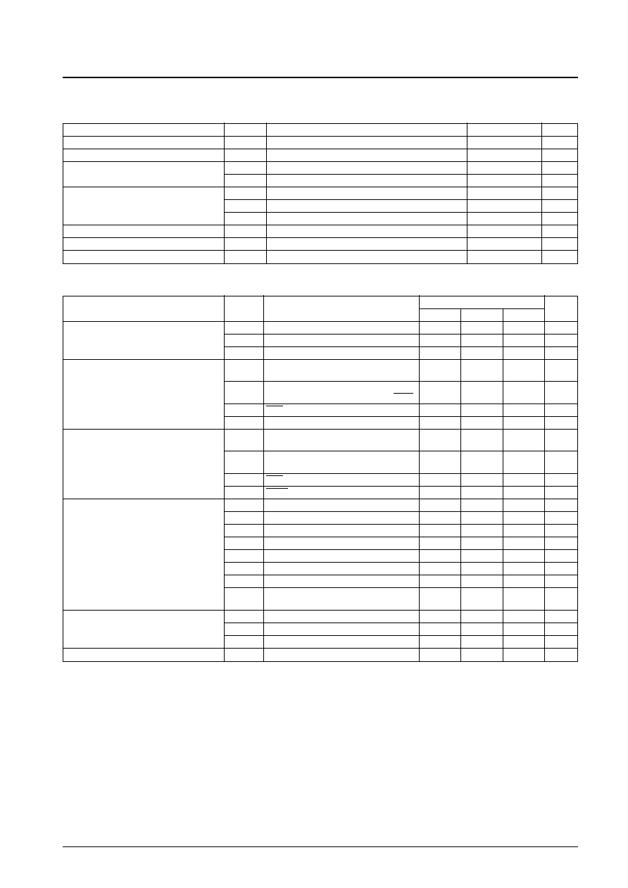
Parameter
Symbol
Conditions
Ratings
Unit
Maximum supply voltage
V
DD
max
≠0.3 to +6.5
V
Input voltage
V
IN
All input pins
≠0.3 to V
DD
+0.3
V
Output voltage
V
OUT
(1)
Port J
≠0.3 to +15
V
V
OUT
(2)
All output ports other than V
OUT
(1)
≠0.3 to V
DD
+0.3
V
I
OUT
(1)
Port J
0 to +5
mA
Output current
I
OUT
(2)
Ports D, E, F, G, K, L, M, N, O, P, and Q, EO1, EO2, EO3, SUBPD
0 to +3
mA
I
OUT
(3)
Ports B and C
0 to +1
mA
Allowable power dissipation
Pd max
Ta = ≠30 to +70∞C
400
mW
Operating temperature
Topr
≠30 to +70
∞C
Storage temperature
Tstg
≠45 to +125
∞C
Specifications
Absolute Maximum Ratings
at Ta = 25∞C, V
SS
= 0 V
Parameter
Symbol
Conditions
Ratings
Unit
min
typ
max
V
DD
(1)
CPU and PLL circuit operating
4.5
5.0
5.5
V
Supply voltage
V
DD
(2)
CPU operating
4.0
5.5
V
V
DD
(3)
Memory retention voltage
1.3
5.5
V
V
IH
(1)
Ports E, H, I, L, M, and Q, HCTR,
0.7 V
DD
V
DD
V
LCTR (when selected for input)
Input high-level voltage
V
IH
(2)
Ports F, G, and K,
0.8 V
DD
V
DD
V
LCTR (in period measurement mode), HOLD
V
IH
(3)
SNS
2.5
V
DD
V
V
IH
(4)
Port A
0.6 V
DD
V
DD
V
V
IL
(1)
Ports E, H, I, L, M, and Q, HCTR,
0
0.3 V
DD
V
LCTR (when selected for input)
Input low-level voltage
V
IL
(2)
Ports A, F, G, and K,
0
0.2 V
DD
V
LCTR (in period measurement mode)
V
IL
(3)
SNS
0
1.3
V
V
IL
(4)
HOLD
0
0.4 V
DD
V
f
IN
(1)
XIN
4.0
4.5
5.0
MHz
f
IN
(2)
FMIN : V
IN
(2), V
DD
(1)
10
150
MHz
f
IN
(3)
FMIN : V
IN
(3), V
DD
(1)
10
130
MHz
f
IN
(4)
AMIN(H) : V
IN
(3), V
DD
(1)
2.0
40
MHz
Input frequency
f
IN
(5)
AMIN(L) : V
IN
(3), V
DD
(1)
0.5
10
MHz
f
IN
(6)
HCTR : V
IN
(3), V
DD
(1)
0.4
12
MHz
f
IN
(7)
LCTR : V
IN
(3), V
DD
(1)
100
500
kHz
f
IN
(8)
LCTR (in period measurement mode):
1
20
◊
10
3
Hz
V
IH
(2), V
IL
(2), V
DD
(1)
V
IN
(1)
XIN
0.5
1.5
Vrms
Input amplitude
V
IN
(2)
FMIN
0.10
1.5
Vrms
V
IN
(3)
FMIN, AMIN, HCTR, LCTR
0.07
1.5
Vrms
Input voltage range
V
IN
(4)
ADI0 to ADI5
0
V
DD
V
Allowable Operating Ranges
at Ta = ≠30 to +70∞C, V
DD
= 3.5 to 5.5 V

No. 5544-5/14
LC72P366
Parameter
Symbol
Conditions
Ratings
Unit
min
typ
max
I
IH
(1)
XIN : V
I
= V
DD
= 5.0 V
2.0
5.0
15
µA
I
IH
(2)
FMIN, AMIN, HCTR, LCTR : V
I
= V
DD
= 5.0 V
4.0
10
30
µA
Ports A, E, F, G, H, I, K, L, M, and Q,
SNS, HOLD, HCTR, LCTR, and with no
Input high-level current
I
IH
(3)
pull-down resistor on port A, V
I
= V
DD
= 5.0 V
3.0
µA
With input mode selected for ports
E, F, G, K, L, M, and Q
I
IH
(4)
Port A: pull-down resistor present
50
µA
I
IL
(1)
XIN:V
I
= V
SS
2.0
5.0
15
µA
I
IL
(2)
FMIN, AMIN, HCTR, LCTR : V
SS
4.0
10
30
µA
Ports A, E, F, G, H, I, K, L, M, and Q,
Input low-level current
SNS, HOLD, HCTR, LCTR, and with no
I
IL
(3)
pull-down resistor on port A, V
I
= V
SS
3.0
µA
With input mode selected for ports E, F,
G, K, L, M, and Q
Input floating voltage
V
IF
Port A: pull-down resistor present
0.05 V
DD
V
Pull-down resistance
R
PD
(1)
Port A: pull-down resistor present V
DD
= 5 V
75
100
200
k
R
PD
(2)
TEST1, TEST2
10
k
Hysteresis
V
H
Ports F, G, and K, LCTR (in period measurement mode)
0.1 V
DD
0.2 V
DD
V
V
OH
(1)
Ports B and C: I
O
= ≠1 mA
V
DD
≠ 2.0
V
DD
≠ 1.0
V
Output high-level voltage
V
OH
(2)
Ports D, E, F, G, K, L, M, N, O, P, and Q: I
O
= ≠1 mA
V
DD
≠ 1.0
V
V
OH
(3)
EO1, EO2, EO3, SUBPD : I
O
= ≠500 µA
V
DD
≠ 1.0
V
V
OH
(4)
XOUT : I
O
= ≠200 µA
V
DD
≠ 1.0
V
V
OL
(1)
Ports B and C: I
O
= 50 µA
1.0
2.0
V
V
OL
(2)
Ports D, E, F, G, K, L, M, N, O, P, and Q: I
O
= 1 mA
1.0
V
Output low-level voltage
V
OL
(3)
EO1, EO2, EO3, SUBPD : I
O
= 500 µA
1.0
V
OL
(4)
XOUT : I
O
= 200 µA
1.5
V
OL
(5)
Port J: I
O
= 5 mA
2.0
V
I
OFF
(1)
Ports B, C, D, E, F, G, K, L, M, N, O, P, and Q
≠3.0
+3.0
µA
Output off leakage current
I
OFF
(2)
EO1, EO2, EO3, SUBPD
≠100
+100
nA
I
OFF
(3)
Port J
≠5.0
+5.0
µA
A/D conversion error
ADI0 to ADI5 : V
DD
(1)
≠1/2
+1/2
LSB
Rejected pulse width
P
REJ
SNS
50
µs
Power down detection voltage
V
DET
3.0
3.5
4.0
V
I
DD
(1)
V
DD
(1) : f
IN
(2) = 130 MHz, Ta = 25∞C
12
24
mA
I
DD
(2)
V
DD
(2): halt mode
*
, Ta = 25∞C (See figure 1.)
0.45
mA
Current drain
I
DD
(3)
V
DD
= 5.5 V, oscillator stopped
5
µA
Ta = 25∞C (See figure 2.)
I
DD
(4)
V
DD
= 2.5 V, oscillator stopped
1
µA
Ta = 25∞C (See figure 2.)
Electrical Characteristics
in the Allowable Operating Ranges
Note:
*
Executing 20 STEP instructions every millisecond. With the PLL and counter circuits stopped.
Note: With PB to PG, and PJ to PQ all open.
However, with PE to PG, PK to PM, and PQ selected for output.
Figure 1 I
DD
(2) in Halt Mode
Note: With PA to PQ all open.
Figure 2 I
DD
(3) and I
DD
(4) in Backup Mode
Test Circuit Diagrams

