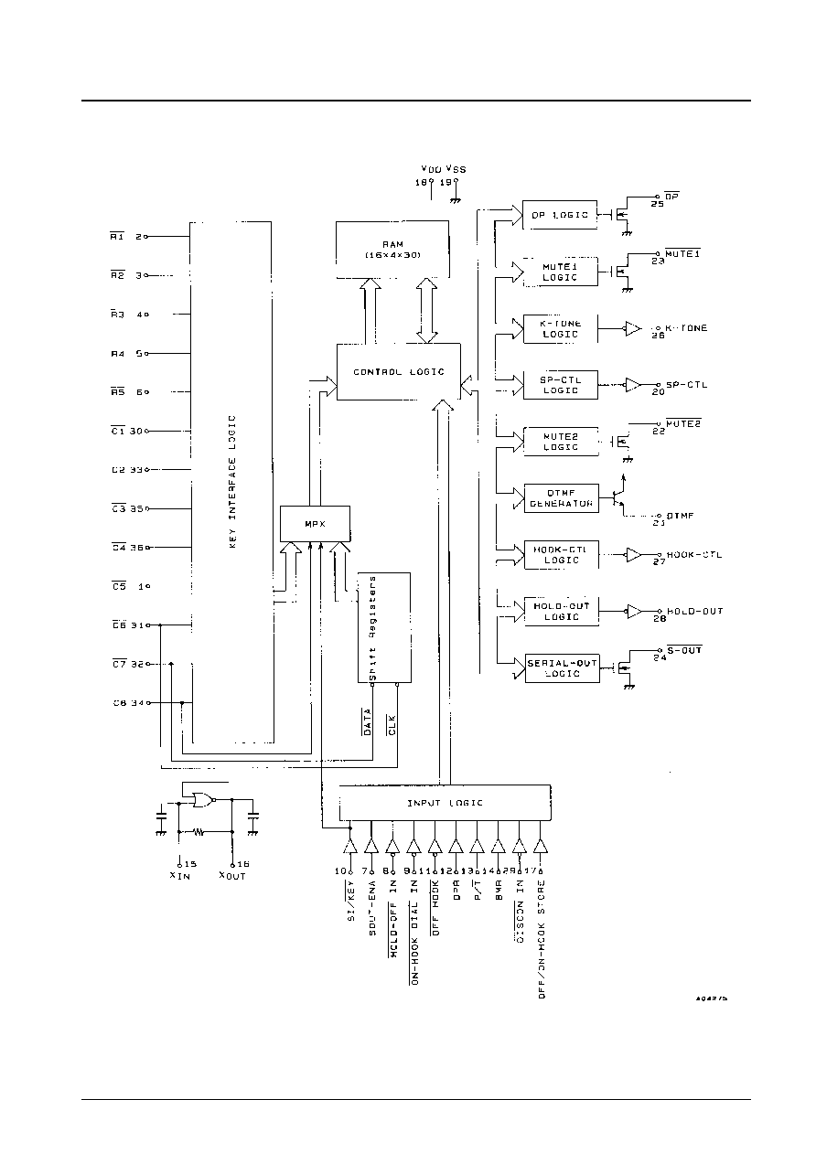
Overview
The LC737212 and LC737212M are CMOS LSI
telephone dialers for pushbutton telephones. They support
both DTMF and pulse dialing. These products include 25
16-digit memories for storing telephone numbers and one
63-digit memory for redialing, and they provide, in a
single chip, all the functions required for dialing and
control for a standard independent telephone, including
on-hook dialing and a hold function. They also provide a
serial I/O interface for connection to a microcontroller.
Functions
∑ Fabrication in a CMOS process that allows these circuits
to be directly operated from a telephone line
∑ Support for single-contact keypads
∑ Built-in oscillator circuit (fosc = 3.58 MHz) that can
drive either a standard color-TV crystal oscillator
element or a ceramic resonator
∑ High-precision DTMF signal
∑ Frequency generator circuit (±0.1%) adopted for eased
ceramic resonator selection
∑ Five one-touch 16-digit auto-dial memories and 20
quick-dialing memories
∑ On-hook or off-hook can be specified for memory
entries.
∑ Mode change and pause data items can be stored in the
dialing memories.
∑ 63-digit redial memory
∑ Automatic pause (3.9 seconds) insertion when the mode
is switched.
∑ Automatic pause (1.0 second) insertion after a flash
operation.
∑ Mode changing is one-directional, from pulse mode to
tone mode.
∑ Output of a key press tone (1036 Hz, 31 ms) for keys
other than DTMF keys when key input is valid
∑ Output of an operation complete confirmation tone
(2072 Hz, 279 ms for each telephone number) when a
telephone number is stored in memory
∑ Generates 12 signal types in DTMF mode.
∑ Supports an on-hook dialing mode.
∑ Supports a hold function with hold mode.
∑ Supports both 10 and 20 pps dialing pulse rates.
∑ The mode can be switched from either the P/T pin or by
a key input.
∑ Settable dialing pulse circuit closed ratio (make
percent): either 33% or 39%.
∑ Supports either keypad or serial input.
∑ Provides serial output of the keypad input data and the
internal status.
∑ Capable of controlling the serial output timing.
∑ Supports 18 user-defined keys.
∑ Wide operating power-supply voltage range
-- Pulse mode: V
DD
= 1.5 to 5.5 V
-- DTMF mode: V
DD
= 2.0 to 5.5 V
∑ Low power operation
-- Pulse mode: I
DD
= 0.5 mA max (V
DD
= 3.0 V)
-- DTMF mode: I
DD
= 1.0 mA max (V
DD
= 3.0 V)
∑ Low standby current
-- I
DR
= 0.5 µA max (V
DD
= 1.0 V)
CMOS LSI
Ordering number : EN5203
203
21398RM(OT) No. 5203-1/27
SANYO Electric Co.,Ltd. Semiconductor Bussiness Headquarters
TOKYO OFFICE Tokyo Bldg., 1-10, 1 Chome, Ueno, Taito-ku, TOKYO, 110-8534 JAPAN
Telephone Dialer IC with On-Chip Memory for Push-
Button Telephones
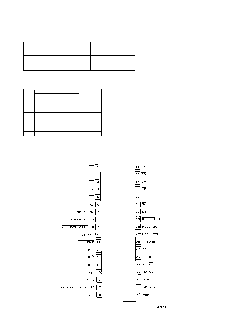
LC737212, LC737212M
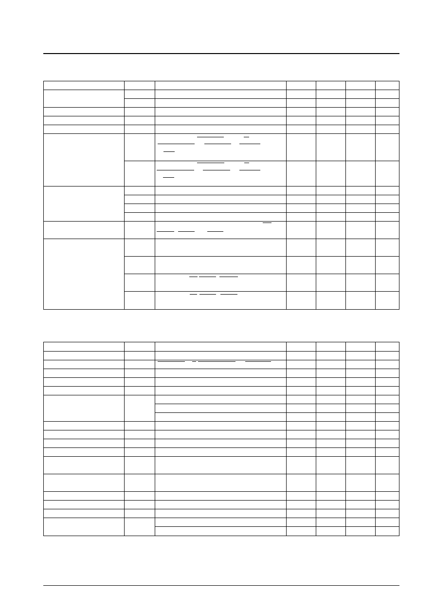
Electrical Characteristics
at Ta = 25∞C, fosc = 3.579545 MHz
AC Characteristics
at Ta = 25∞C, fosc = 3.579545 MHz
No. 5203-3/27
LC737212, 737212M
Parameter
Symbol
Conditions
min
typ
max
Unit
Operating current drain
I
DDP
Pulse output mode, outputs open, V
DD
= 3.0 V
0.3
0.5
mA
I
DDT
DTMF output mode,outputs open, V
DD
= 3.0 V
0.5
1
mA
Static current drain
I
DD(ST)
Standby mode, outputs open, V
DD
= 1.5 to 5.5 V
1
µA
Memory retention voltage
V
DR
Between V
DD
and V
SS
1
V
Memory retention current
I
DR
V
DD
= 1 V
0.5
µA
The SOUT-ENA, OFF-HOOK, DPR, P/T, BMR,
I
IH1
ON-HOOK-DIAL IN, HOLD-OFF IN, DISCON IN,
1
µA
Input pin current
SI/KEY, OFF/ON-HOOK, and STORE pins, V
IH
= V
DD
The SOUT-ENA, OFF-HOOK, DPR, P/T, BMR,
I
IL1
ON-HOOK-DIAL IN, HOLD-OFF IN, DISCON IN,
≠1
µA
SI/KEY, OFF/ON-HOOK, and STORE pins, V
IL
= V
SS
I
ILK1
All key pins, V
DD
= 1.5 V, V
ILK
= V
SS
≠20
µA
I
ILK2
All key pins, V
DD
= 5.5 V, V
ILK
= V
SS
≠300
µA
Key pin current
I
OLK1
All key pins, V
DD
= 1.5 V, V
OLK
= 0.4 V
200
µA
I
OLK2
All key pins, V
DD
= 5.5 V, V
OLK
= 0.4 V
0.7
mA
Output pin leakage current
I
OFF
V
O
= V
DD
, V
DD
= 5.5 V, with the output off, the DP,
1
µA
MUTE1, MUTE2, and S-OUT pins.
V
OH1
The K-TONE, HOLD-OUT, HOOK-CTL,
V
DD
≠ 0.5
V
and SP-CTL pins, V
DD
= 1.5 V, I
OH
= ≠250 µA
V
OH2
The K-TONE, HOLD-OUT, HOOK-CTL,
V
DD
≠ 1
V
Output pin voltage
and SP-CTL pins, V
DD
= 5.5 V, I
OH
= ≠1 mA
V
OL1
The K-TONE, DP, MUTE1, MUTE2, SP-CTL,
0.4
V
HOLD-OUT, and HOOK-CTL pins, V
DD
= 1.5 V, I
OL
= 250 µA
V
OL2
The K-TONE, DP, MUTE1, MUTE2, SP-CTL,
0.4
V
HOLD-OUT, and HOOK-CTL pins, V
DD
= 5.5 V, I
OL
= 1 mA
Parameter
Symbol
Conditions
min
typ
max
Unit
Key debounce time
T
KD
30
ms
Pin chatter exclusion time
T
PCHT
OFF-HOOK, P/T, ON-HOOK-DIAL, IN HOLD OFF IN
45
ms
Key scan frequency
f
KSC
258.9
HZ
Key tone frequency
f
KT
1035.7
HZ
Key tone output time
T
KT
30.9
ms
In Pulse mode at 10 pps
3.88
3.9
3.93
s
Auto-pause time
T
AP
In Pulse mode at 20 pps
3.88
3.9
3.93
s
DTMF mode
3.88
3.9
3.93
s
DTMF output time
T
MFON
98
100
102
ms
DTMF interdigit pause time
T
MFOFF
93
95
97
ms
Hooking time
T
HK
700
710
720
ms
Hooking pause time
T
HKP
0.98
1.0
1.02
s
Memory store confirmation
f
KST
2071.4
Hz
tone frequency
Memory store confirmation
T
KSTON
278.1
ms
tone output time
Low tone amplitude
V
OR
V
DD
= 3.5 V, R
L
= 10 k
165
200
240
mVrms
Tone output ratio
dBCR
V
DD
= 2.0 to 5.5 V, R
L
= 10 k
1
2
3
dB
Tone output distortion
DIS
V
DD
= 2.0 to 5.5 V, R
L
= 10 k
10
%
Oscillator start time
T
START
V
DD
= 1.5 to 5.5 V
30
ms
V
DD
= 3.0V
1
ms