91400 RM (IM) Ohta No.6685-1/16
Ver.1.03
90699
Preliminary
Overview
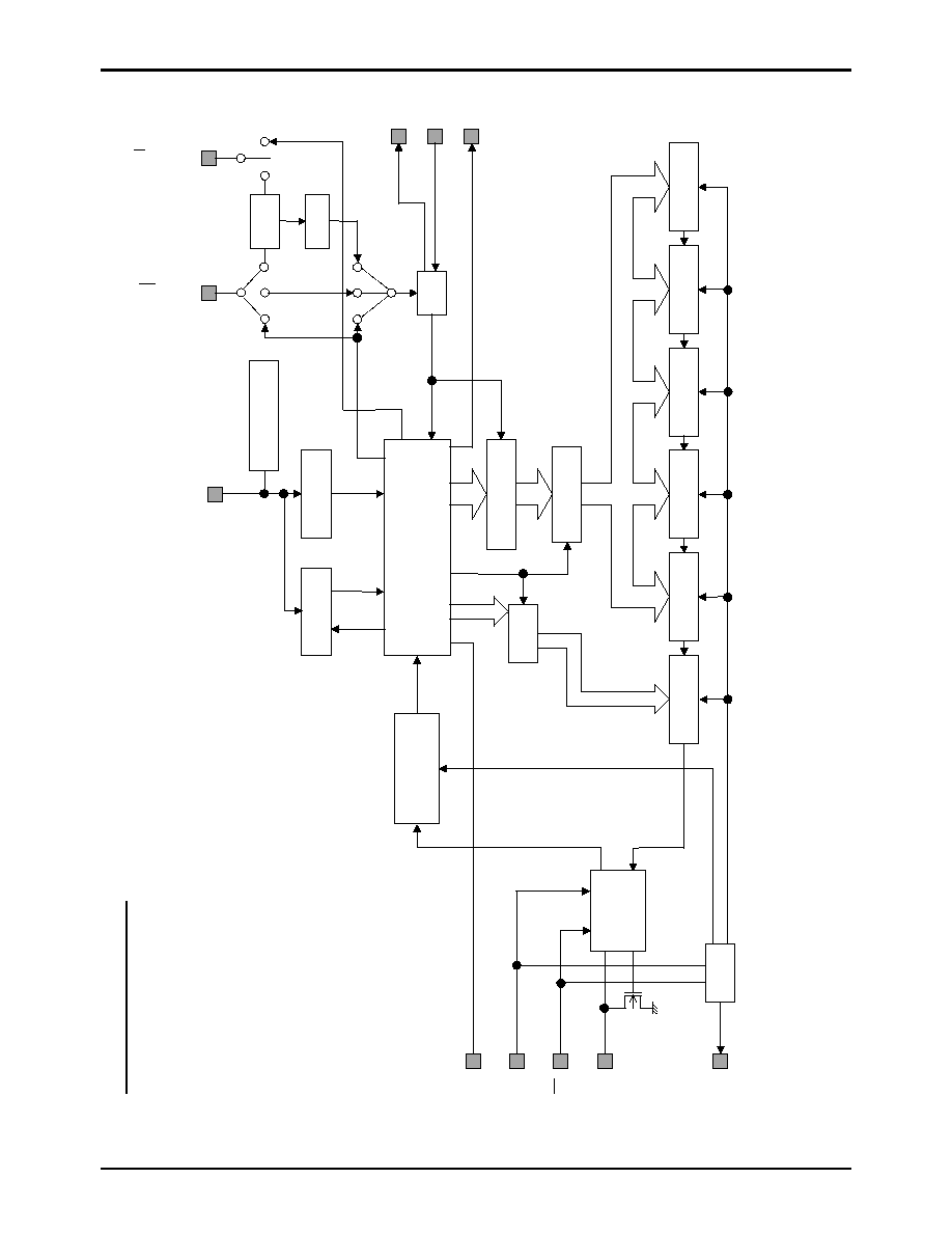
The LC7454A/M is a data slicer IC for the Index Plus + signals. The LC7454A/M extracts the Caption and the Index Plus +
data form the Vertical Blanking Period of the TV signal and send it out to the decoder IC (Usually Microcomputer).
The LC7454A/M can be used to extract the Closed Caption signals, the XDS signals and the Index Plus + signals.
Features
(1) Low power dessipation by CMOS process
(2) Stable signal extraction by integrated peak hold circuit and digital circuit.
(3) Operation Voltage range
: 5V ± 10%
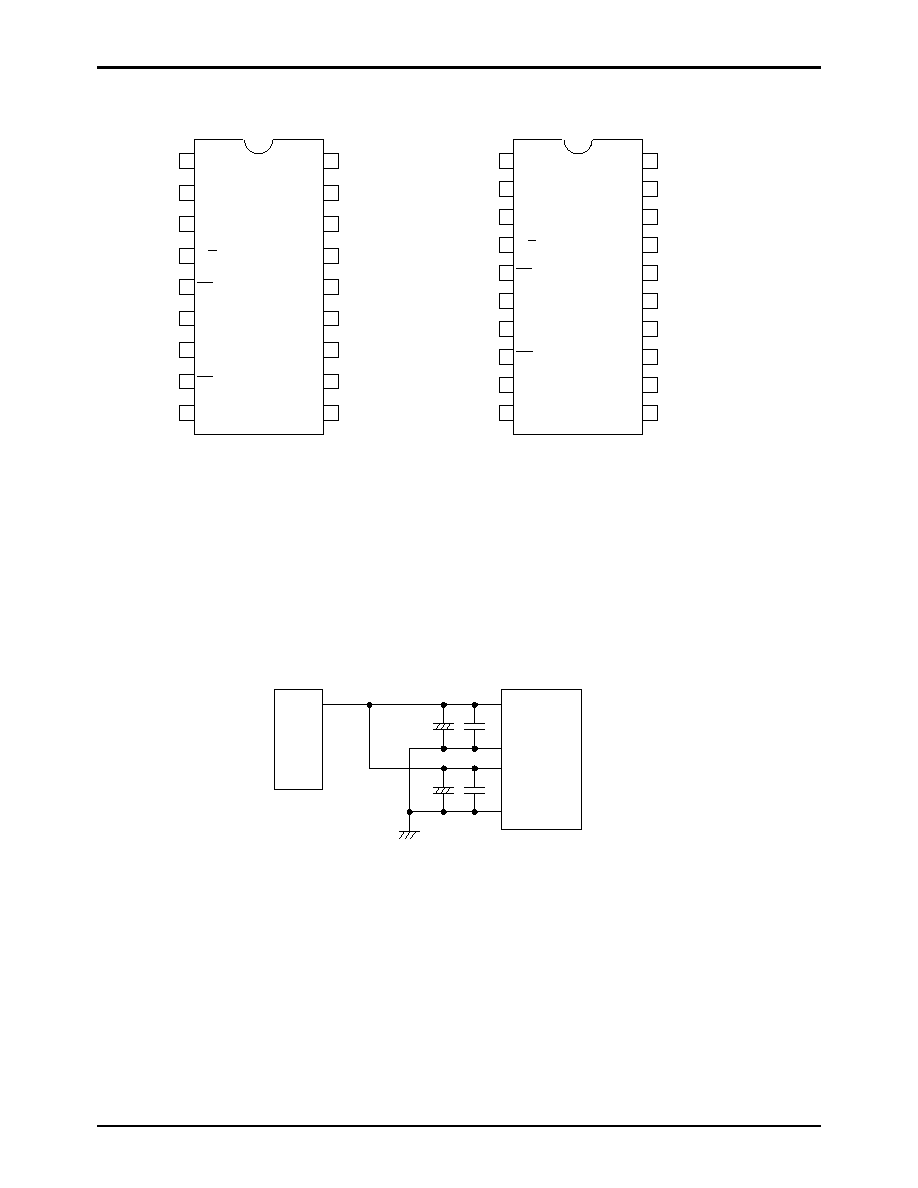
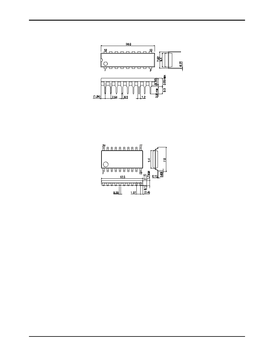
(4) Package
LC7454A : DIP18
LC7454M : MFP20
CMOS Data Slicer
LC7454A/M
Ordering number : ENN*6685
CMOS IC
LC7454A/M
No.6685-5/16
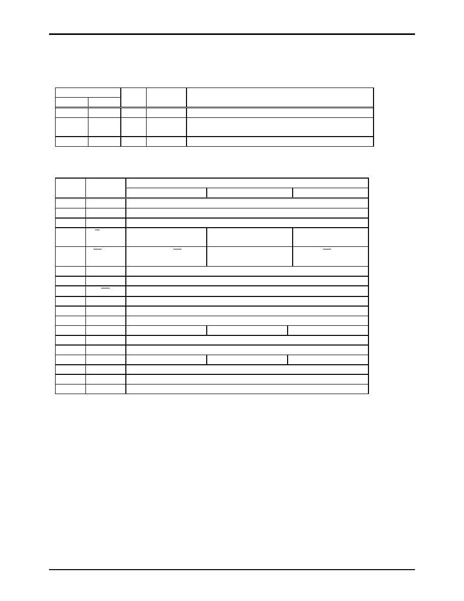
Operation on each mode
The LC7454 has three operating modes. The operation mode be selected by the status of MOD0 and MOD1 terminals. The functionality of
three modes are the same. Only the PLL reference frequency which is used to generate operation clock is different. Use mode1 or mode3
only in the application which uses 2x data. Any mode (Mode1,2 or 3) can be used in the 1x data only application.
Terminal
MOD1 MOD0
MODE Applications
PLL
reference
Open
Open
Mode1 NTSC-VCR Use H-sync signal which is separated from C-Video signal.
Open
VDD1
Mode2 NTSC-VCR Use 1/32 divided signal 503 KHz which is generated by external
ceramic resonator.
VDD
Open
Mode3
NTSC-TV
Use H-sync signal from Fly Back.
Terminal Functions
Function Description
Terminal #
(DIP18)
Terminal
name
Mode 1
Mode 2
Mode 3
1 VSS1
Ground
2
TEST
Test terminal, Open in normal operation
3 LN26
32
µ
s Pulse output at line 26 timing on both field
4
O/ E /CFOUT Pulse output for field
judgment
*1
Output terminal for ceramic
resonator
Pulse output for field
judgment
*1
5
HS
/CFIN Sync
separated
HS
pulse
output
Input terminal for Ceramic
resonator
External HS pulse input
6
DATA
Line select data input and slice data output
*2
7
SCKIN
Data transmit clock input
8
CE
Chip select input
*3
9
IOC
Data direction control signal input
*4
10
SLICE
Pulse output at selected slice line
11 VDD1
Power
terminal
12
MOD0
Open
Connect to VDD
Open
13 CVIN
Conposit
video
input
14
VCOR
Connect resister for internal VCO oscillation frequency control
15
MOD1
Open Open Connect
to
VDD
16 VDD2
Power
terminal
17 VSS2
Ground
18
CP
Filter terminal for internal PLL
*1 `H' level in Odd field, `L' level in Even field.
*2 N-ch open drain in output mode.
*3 Feed `L' level only when data transmission is in effect. If CE='H', data terminal will become
input/output disable, SCKIN terminal will become input disable.
*4 `H' level : Output mode
`L' level : Input mode