 | –≠–ª–µ–∫—Ç—Ä–æ–Ω–Ω—ã–π –∫–æ–º–ø–æ–Ω–µ–Ω—Ç: LC7455 | –°–∫–∞—á–∞—Ç—å:  PDF PDF  ZIP ZIP |
Ordering number : EN5680
D3097HA(OT) No. 5680-1/13
Overview
The LC7455A/M extracts the closed caption signal
superimposed on a video signal during the vertical return
period and, under the control of a clock signal provided by
the decoder IC, transfers that signal to the IC (usually a
microcontroller) that decodes the closed caption data. The
LC7455A/M supports four operating modes. Modes 1 and
2 can be used for XDS. In these modes, the LC7455A/M,
in combination with the decoder IC (microcontroller),
extracts the caption signal superimposed on field 2 and
uses it for NTSC VCR functions such as the automatic
time and date setting function. In modes 3 and 4, the
LC7455A/M, in combination with the decoder IC
(microcontroller), extracts the caption signal
superimposed on fields 1 and 2 and uses it for NTSC TV
applications (mode 3) or PAL TV applications (mode 4).
Functions
∑ Low power dissipation achieved by fabrication in a
CMOS process.
∑ Stable caption signal extraction achieved by a built-in
peak hold circuit and the use of digital technology.
∑ Operating supply voltage: 5 V ±10%
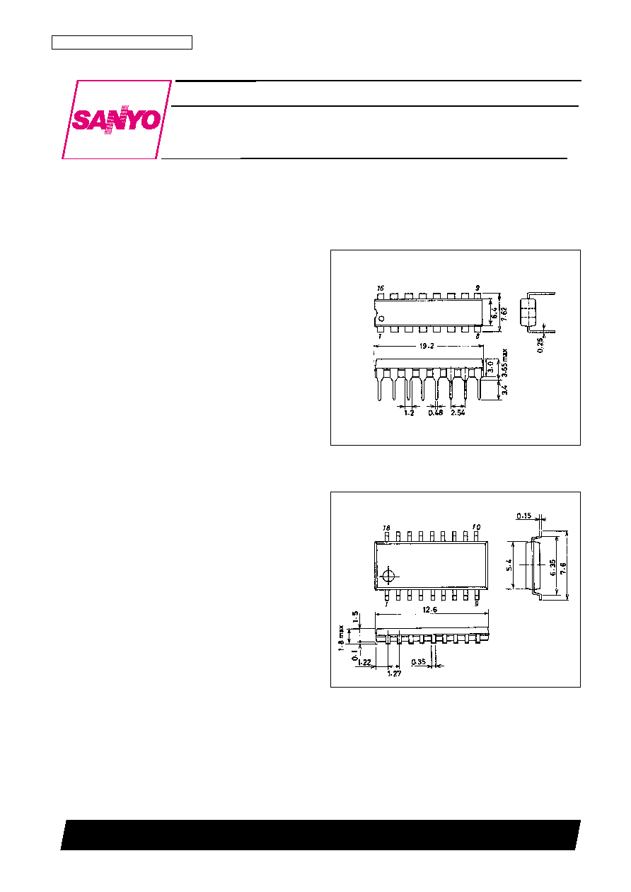
∑ Package
LC7455A: 16-pin DIP
LC7455M: 18-pin MFP
Package Dimensions
unit: mm
3006B-DIP16
unit: mm
3095-MFP18
SANYO: DIP16
[LC7455A]
SANYO: MFP18
[LC7455M]
LC7455A, 7455M
SANYO Electric Co.,Ltd. Semiconductor Bussiness Headquarters
TOKYO OFFICE Tokyo Bldg., 1-10, 1 Chome, Ueno, Taito-ku, TOKYO, 110 JAPAN
Closed Caption Signal Extraction IC
CMOS IC
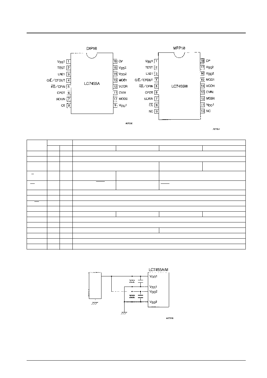
Pin Assignments
Note: V
DD
1 and V
SS
1 are the power supply for the digital block, and V
DD
2 and V
SS
2 are the power supply for the analog block. Use a circuit similar to the
one shown below to minimize mutual interference due to noise from these blocks.
No. 5680-2/13
LC7455A, 7455M
Pin Functions
Pin
Pin No.
Pin function
DIP16
MFP18
Mode 1
Mode2
Mode3
Mode4
V
SS
1
1
1
Ground
TEST
2
2
Test pin. Must be left open during normal operation.
LN21
3
3
Line 21H pulse output (even field)
Line 21H pulse output
Line 22H pulse output
(both fields)
(both fields)
O/E/CFOUT
4
4
Field discrimination pulse
Ceramic oscillator output
Field discrimination pulse output
output
HS/CFIN
5
5
Sync separator Hsync
Ceramic oscillator input
Hsync pulse input
pulse output
CPDT
6
6
Caption data output (n-channel open-drain output)
SCKIN
7
7
Caption data transfer clock input
CE
8
8
Chip select input
V
DD
1
9
11
Power supply
MOD0
10
12
Leave open
Short to the power supply
Leave open
Short to the power supply
CVIN
11
13
Composite video input
VCOR
12
14
Connection for an external resistor to control the built-in VCO oscillator frequency
MOD1
13
15
Leave open
Short to the power supply
V
DD
2
14
16
Power supply
V
SS
2
15
17
Ground
CP
16
18
Connection for the filter used by the built-in PLL
Power
supply
Top view

System Block Diagram
No. 5680-3/13
LC7455A, 7455M
Operation in the Different Modes
Pin
Application
Mode
equipment
Operation
MOD1
MOD0
∑ Even field line 21 data extraction
Open
Open
Mode 1
VCR
The internal PLL is operated with the horizontal synchronizing signal separated from the composite video
signal as the reference.
∑ Even field line 21 data extraction
Open
V
DD
Mode 2
VCR
An external 508 kHz ceramic oscillator is used, and the internal PLL is operated with that oscillator output
divided by 32 as the reference.
V
DD
Open
Mode 3
NTSC-TV
∑ Odd and even field line 21 data extraction
The internal PLL is operated with the Hsync signal applied from fly back as the reference.
V
DD
V
DD
Mode 4
PAL-TV
∑ Odd and even field line 22 data extraction
The internal PLL is operated with the Hsync signal applied from the fly back circuit as the reference.
Note: The data extraction operations in modes 1 and 2 are identical. However, while mode 1 can operate without problem for normal "on air" signals, it may
be difficult for the PLL to lock with signals such as scrambled CATV signals.
PLL reference clock
mode 2
mode 3, 4
mode 1
Data peak hold
(Data slice)
Hsync peak hold
(Hsync slice)
Output control
Data output
buffer
Divided-by-
32 circuit
Oscillator
circuit
Pedestal clamp
(Mode 2)
(Mode 2)
(Modes 1, 3, 4)
No. 5680-4/13
LC7455A, 7455M
Parameter
Symbol
Conditions
Ratings
Unit
Maximum supply voltage
V
DD
max
V
DD
1, V
DD
2: V
DD
1 = V
DD
2
≠0.3 to +7.0
V
Input voltage
V
I
HS/CFIN, CVIN, SCKIN, CE
≠0.3 to V
DD
+0.3
V
Output voltage
V
O
LN21, CPDT, O/E/CFOUT, HS/CFIN
≠0.3 to V
DD
+0.3
V
Allowable power dissipation
Pd max
LC7455A
300
mW
LC7455M
150
mW
Operating temperature
Topr
≠30 to +70
∞C
Storage temperature
Tstg
≠55 to +150
∞C
Specifications
Absolute Maximum Ratings
at Ta = 25∞C, V
SS
= 0 V
Note: V
SS
1 and V
SS
2 must be at the same potential.
V
DD
1 and V
DD
2 must be at the same potential.
Parameter
Symbol
Conditions
Ratings
Unit
min
typ
max
Operating supply voltage
V
DD
V
DD
1, V
DD
2 : V
DD
1 = V
DD
2
4.5
5.5
V
Input high-level voltage
V
IH
HS/CFIN, SCKIN, CE;
0.75 V
DD
V
DD
V
V
DD
= 4.5 to 5.5 V
Input low-level voltage
V
IL
HS/CFIN, SCKIN, CE;
V
SS
0.25V
DD
V
V
DD
= 4.5 to 5.5 V
CVIN input amplitude
CVSYNC
CVIN : SYNC-WHITE = 1.0 V;
1Vp-p ≠ 3dB
1Vp-p
1Vp-p + 3 dB
V
V
DD
= 4.5 to 5.5 V
HS/CFIN : V
DD
= 4.5 V
HS input frequency range
f
H
For mode 3
15.23
15.73
16.23
kHz
For mode 4
15.13
15.63
16.13
kHz
HS/CFIN, O/E/CFOUT;
Oscillator frequency range
*
1
FmCF
For mode 2, see Figure 1.
503
508
513
kHz
V
DD
= 4.5 to 5.5 V
HS/CFIN, O/E/CFOUT;
Oscillator stabilization time
*
2
tmsCF
For mode 2, see Figure 2.
0.5
5
ms
V
DD
= 4.5 to 5.5 V
Allowable Operating Ranges
at Ta = ≠30 to +70∞C, V
SS
= 0 V
Parameter
Symbol
Conditions
Ratings
Unit
min
typ
max
Input high-level current
I
IH
HS/CFIN, SCKIN, CE : V
IN
= V
DD
;
1
µA
V
DD
= 4.5 to 5.5 V
Input low-level current
I
IL
HS/CFIN, SCKIN, CE : V
IN
= V
SS
;
≠1
µA
V
DD
= 4.5 to 5.5 V
Output high-level voltage
V
OH
LN21, O/E/CFOUT, HS/CFIN;
V
DD
≠ 1.2
V
I
OH
= ≠4 mA ; V
DD
= 4.5 to 5.5 V
Output low-level voltage
V
OL
LN21, CPDT, O/E/CFOUT,
1
V
HS/CFIN : I
OL
= 10 mA; V
DD
= 4.5 to 5.5 V
Input clamping voltage
V
CLMP
CVIN ; V
DD
= 5.0 V
2.3
2.5
2.7
V
Input clamping current
I
IC
CVIN : CVIN = 3 V ; V
DD
= 5.0 V
5
10
18
µA
Output clamping current
I
OC
CVIN : CVIN = 2 V ; V
DD
= 5.0 V
≠120
≠70
≠30
µA
Current drain
I
DD
V
DD
1, V
DD
2 ; V
DD
= 4.5 to 5.5 V
6
15
mA
Electrical Characteristics
at Ta = ≠30 to +70∞C, V
SS
= 0 V.
Note: 1. See Table 1 for more information on the oscillator frequency.
2. The oscillator stabilization time is the time required until the oscillator is stable after the power-supply voltage is applied. See figure 2.
Parameter
Symbol
Conditions
Ratings
Unit
min
typ
max
[Serial clock]
Input clock period
t
CKCY
SCKIN : See Figure 3.
1
µs
Input clock low-level pulse width
t
CKL
SCKIN : See Figure 3.
0.5
µs
Input clock high-level pulse width
t
CKH
SCKIN : See Figure 3.
0.5
µs
Setup time
t
ICK
SCKIN : Stipulated with respect to the falling
1
µs
edge of CE.
[Serial output]
Output delay time
t
CKO
0.5
µs
Serial Output Characteristics
at Ta = ≠30 to +70∞C, V
SS
= 0 V, V
DD
= 4.5 to 5.5 V
Stipulated with respect to the falling edge of
SCKIN. A 1-k
external pull-up resistor is
connected. See Figure 3.

No. 5680-5/13
LC7455A, 7455M
Table 1 Ceramic Oscillator Guaranteed Constants
Figure 1 Ceramic Oscillator
Figure 2 Oscillator Stabilization Time
Figure 3 Serial Output Test Conditions
Note: Capacitors with K tolerance (±10%) and SL characteristics must be used for C1 and C2.
∑ Since this circuit is influenced by the length of the circuit pattern, components related to oscillator functioning must be mounted as close together as
possible so that pattern lines do not become longer than is absolutely necessary.
∑ The characteristics are not guaranteed if an oscillator element other than the one listed above is used.
Oscillator type
Manufacturer
Oscillator element
C1
C2
508-kHz ceramic oscillator
Murata Mfg. Co., Ltd.
CSB 508E
150 pF
150 pF
Power supply
Operating V
DD
lower limit
<AC timing measurement point>
<Timing>
<Test load>
Note: CPDT goes to the high-impedance state while CE is high.