LC7456A
No.6733-1/6
Overview
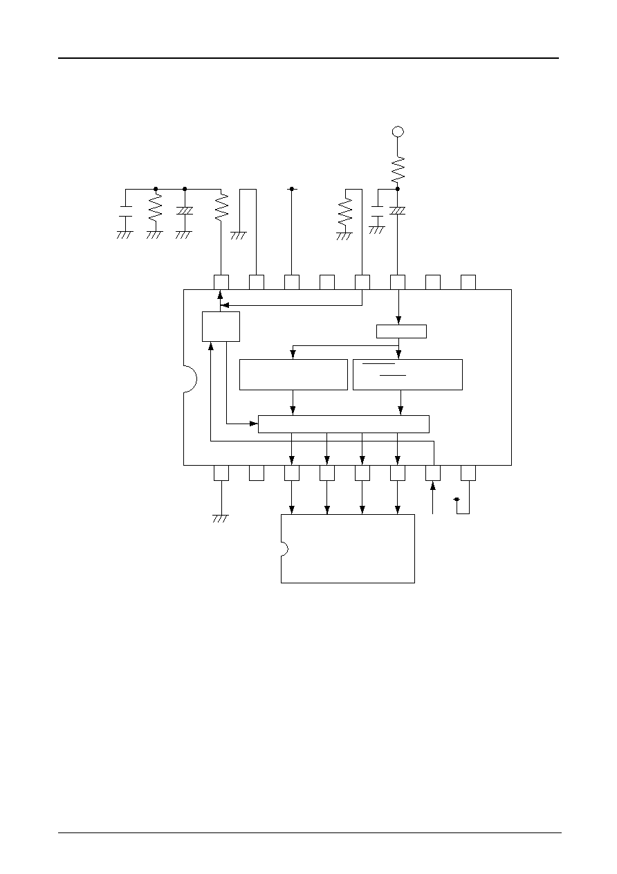
The LC7456A receives the composite video signal from the V / C (Video Chroma) signal processor and extracts the
closed caption data. This data and a clock signal, generated by an on-chip PLL, are then sent to the decoder IC. The
LC7456A is a CMOS version of the LA7945 IC also currently in production. The differences between the LA7945 and
the LC7456A are a change from Bipolar to CMOS technology, a smaller package size (22 pins to 16 pins), and a
reduction in the external circuitry requierd.
An LC8640XX series microcontroller is needed to perform the decoding after the LC7456A has extracted the caption
data from the composite video signal.
Features
∑ Low power consumption due to CMOS process
∑ Accurate caption signal extraction using a built-in pead hold circuit and digital technology.
∑ Power Requirement : 5V
±
10 %
∑ Package : DIP16
SANYO Electric Co.,Ltd. Semiconductor Company
TOKYO OFFICE Tokyo Bldg., 1-10, 1 Chome, Ueno, Taito-ku, TOKYO, 110-8534 JAPAN
Ordering number : ENN*6733
LC7456A
U.S. Closed Caption Signal Extraction IC
D2000 RM (IM) O
Any and all SANYO products described or contained herein do not have specifications that can handle
applications that require extremely high levels of reliability, such as life-support systems, aircraft's
control systems, or other applications whose failure can be reasonably expected to result in serious
physical and/or material damage. Consult with your SANYO representative nearest you before using
any SANYO products described or contained herein in such applications.
SANYO assumes no responsibility for equipment failures that result from using products at values that
exceed, even momentarily, rated values (such as maximum ratings, operating condition ranges, or other
parameters) listed in products specifications of any and all SANYO products described or contained
herein.
CMOS IC
Ver. 1.02B
21594
Preliminary
LC7456A
No.6733-2/6
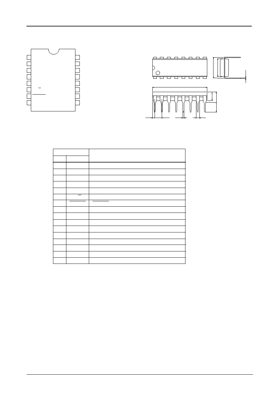
Pin Arrangement Diagram (DIP16)
Pin Function
Pin
Function
No.
Name
1
VSS1
GND
2
TEST1
Test pin, usually open
3
LN21
Line 21H pulse output
4
CPDT
Caption data output
5
CPCK
Caption data latch clock output
6
O/E
Field determination output
7
HSYNC
HSYNC input
8
VDD1
Power supply
9
SILCE
Caption data slice level output
10
PEAK
Caption data peak hold level output
11
CVIN
Composite video input
12
VCOR
Built-in VCO frequency control pin
13
TEST2
Test pin, usually open
14
VDD2
Power supply
15
VSS2
GND
16
CP
Built-in PLL filter pin
1
2
3
4
5
6
7
8
16
15
14
13
12
11
10
9
CP
VSS2
VDD2
TEST2
VCOR
CVIN
PEAK
SLICE
VSS1
TEST1
LN21
CPDT
CPCK
VDD1
O / E
HSYNC
ILC00006
1
8
16
9
3.0
3.4
3.65max
19.2
0.71
2.54
1.2
0.25
0.48
7.62
6.4
Package Dimensions
unit : mm
3006B
SANYO : DIP16(300mil)
LC7456A
No.6733-4/6
1. Absolute Maximum Ratings
at VSS=0V and Ta=25
∞
C
Parameter
Symbol
Pins
Conditions
Ratings
min.
typ.
max.
unit
Supply voltage
VDDMAX VDD1, VDD2
VDD1=VDD2
-- 0.3
+7.0
V
Input voltage
VI
HSYNC, CVIN
-- 0.3
VDD+0.3
Output voltage
VO
LN21, CPDT
-- 0.3
VDD+0.3
CPCK, O / E
Maximum
Pdmax
DIP16
300
mW
power
dissipation
Operating
Topr
-- 30
+70
∞
C
temperature
range
Storage
Tstg
-- 55
+150
temperature
range
* VSS1 and VSS2 are same level.
VDD1 and VDD2 are also same level.
2. Recommended Operating Range
at VSS=0V and Ta= -- 30
∞
C to +70
∞
C
Parameter
Symbol
Pins
Conditions
Ratings
VDD[V]
min.
typ.
max.
unit
Operating
VDD
VDD1,VDD2
VDD1=VDD2
4.5
5.5
V
supply voltage
Input high
VIH
HSYNC
4.5 to 5.5 0.85VDD
VDD
voltage
Input low
VIL
HSYNC
4.5 to 5.5
VSS
0.25VDD
voltage
CVIN analog
CVSYNC
CVIN
SYNC-WHITE=1.0V 4.5 to 5.5 1Vp-p-3dB
1Vp-p
1Vp-p+3dB
input range
HSYNC input
fH
HSYNC
4.5 to 5.5
15.60
15.73
15.90
KHz
frequency range
3. Electrical Characteristics
at VSS=0V and Ta= -- 30
∞
C to +70
∞
C
Parameter
Symbol
Pins
Conditions
Ratings
VDD[V]
min.
typ.
max.
unit
Input high
IIH
HSYNC
VIN=VDD
4.5 to 5.5
1
µ
A
current
Input low
IIL
HSYNC
VIN=VSS
4.5 to 5.5
-- 1
current
Output high
VOH
LN21, CPDT
IOH= -- 4mA
4.5 to 5.5 VDD-1.2
V
voltage
CPCK, O / E
Output low
VOL
LN21, CPDT
IOL=10mA
4.5 to 5.5
1
voltage
CPCK, O / E
Input clamp
VCLMP
CVIN
5.0
2.3
2.5
2.7
voltage