 | –≠–ª–µ–∫—Ç—Ä–æ–Ω–Ω—ã–π –∫–æ–º–ø–æ–Ω–µ–Ω—Ç: LC7461M | –°–∫–∞—á–∞—Ç—å:  PDF PDF  ZIP ZIP |
Infrared Remote Control Transmitter IC
Functions
.
32
%3 function keys
.
13-bit custom codes
.
Operating supply voltage range V
DD
= 1.8 to 3.6 V
.
Supply current at the standby mode I
DD
= 1 µA or less
.
Double-press operation keys (no priority given)
.
On-chip oscillator (ceramic resonator : connected externally)
Features
.
The custom code consists of 7 bits to be fixed by the
on-chip ROM and 6 bits being pin-settable. Sixty-four
custom codes may be selected externally (no diode required).
.
Minimum number of external parts required
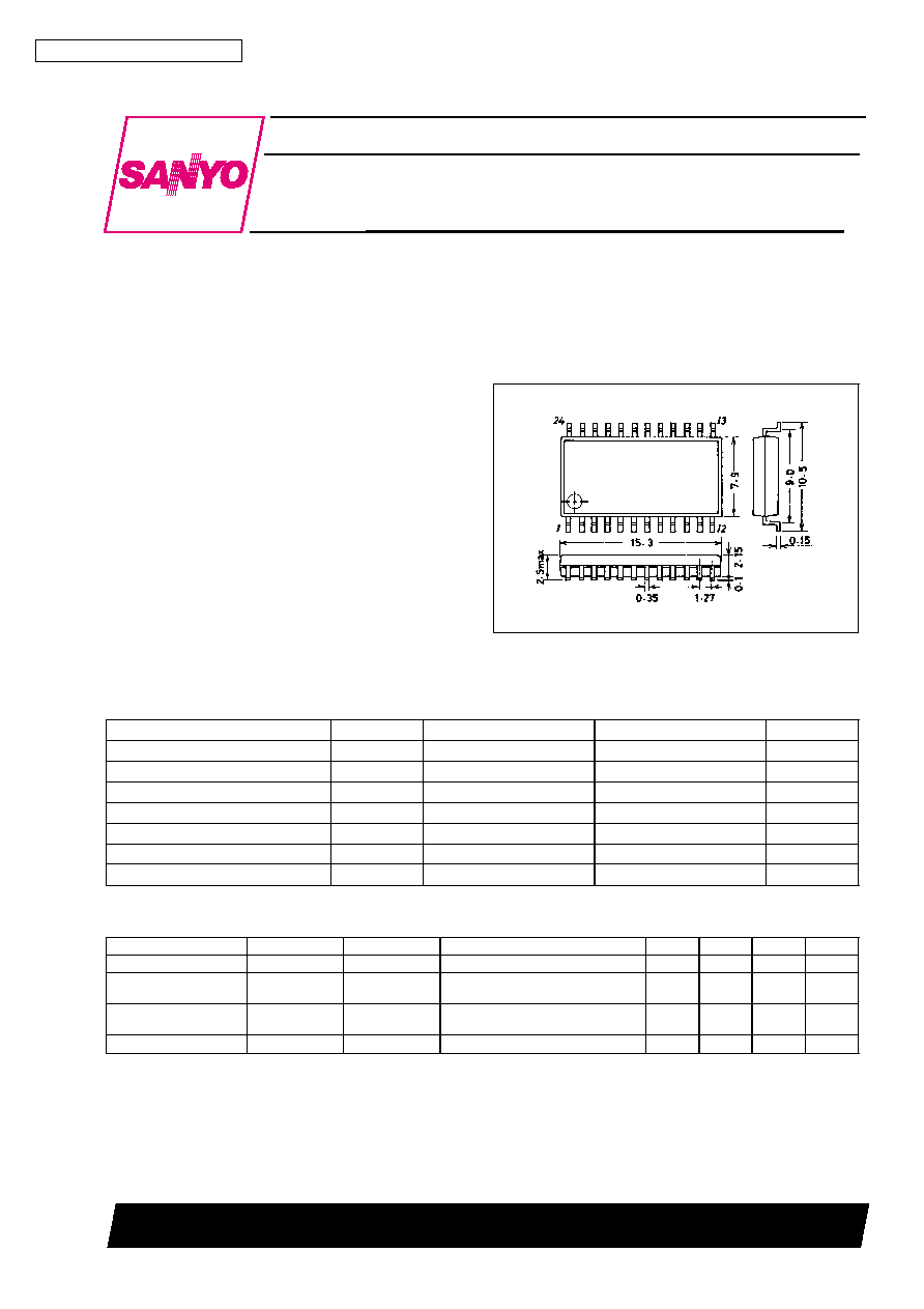
Package Dimensions
unit : mm
3045B-MFP24
[LC7461M]
SANYO : MFP24
Specifications
Absolute Maximum Ratings
at Ta = 25∞C
Parameter
Symbol
Conditions
Ratings
Unit
Maximum supply voltage
V
DD
max
V
DD
V
SS
≠0.3 to +5.5
V
Input voltage
V
IN
Each input pin
V
SS
≠0.3 to V
DD
+0.3
V
Output voltage
V
OUT
Each output pin
V
SS
≠0.3 to V
DD
+0.3
V
Output current
I
OUT
OUT
≠35
mA
Allowable power dissipation
Pd max
Ta
%
85∞C
150
mW
Operating temperature
Topr
≠40 to +85
∞C
Storage temperature
Tstg
≠50 to +125
∞C
Allowable Operating Conditions
at Ta = 25∞C
Parameter
Symbol
Pin Name
Conditions
min
typ
max
Unit
Supply voltage
V
DD
V
DD
f
OSC
= 455 kHz
1.8
3.0
3.6
V
Input high-level voltage
V
IH
K
I
0 to K
I
3,
C
0
to C
5
0.7 V
DD
V
DD
V
Input low-level voltage
V
IL
K
I
0 to K
I
3,
C
0
to C
5
V
SS
0.3V
DD
V
Oscillation frequency
f
OSC
400
455
500
kHz
Ordering number: EN2119D
CMOS LSI
LC7461M
SANYO Electric Co.,Ltd. Semiconductor Bussiness Headquarters
TOKYO OFFICE Tokyo Bldg., 1-10, 1 Chome, Ueno, Taito-ku, TOKYO, 110 JAPAN
O3096HA(II)/7058YT/6036KI,TS(KOTO) No.2119-1/7
Electrical Characteristics
at Ta = 25∞C, V
DD
= 3.0 V
Parameter
Symbol
Pin Name
Conditions
min
typ
max
Unit
Operating supply
current
I
DD
V
DD
Key ON, output: no load
1
mA
Quiescent supply
current
I
DS
V
DD
All keys OFF, OSC stop
1
µA
Output high-level
current
I
OH
1
OUT
V
DD
= 1.8 V, V
OH
= 1.0 V
≠8
mA
I
OH
2
OUT
V
DD
= 3.0 V, V
OH
= 1.0 V
≠25
mA
Output high-level
voltage
V
OH
K
O
0 to K
O
7
I
OH
= ≠0.1 mA
0.3
V
Output low-level
voltage
V
OL
OUT
I
OL
= 0.1 mA
0.3
V
Output OFF-state
leakage current
I
OFF
K
O
0 to K
O
7
1
µA
Input high-level current
I
IH
C
0
to C
5
V
IN
= V
DD
1
µA
Input low-level current
I
IL
C
0
to C
5
V
IN
= V
SS
≠1
µA
Input floating voltage
V
IF
K
I
0 to K
I
3
0.1 V
DD
V
Input pull down
resistance
R
IN
K
I
0 to K
I
3
75
100
125
k
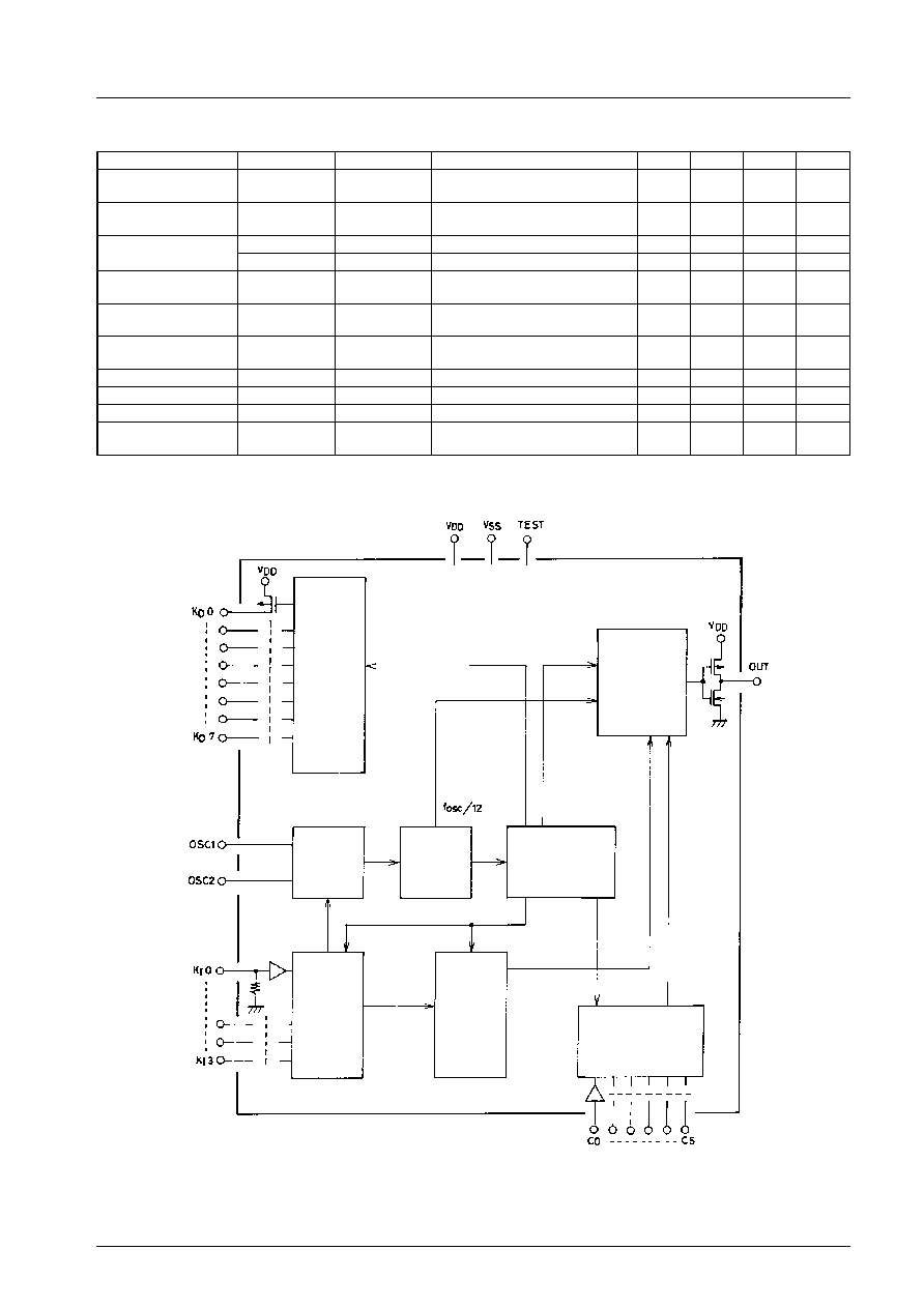
Internal Block Diagram
Key
output
timing
signal
generator
Output
circuit
Oscillator
Divider
Decoder
Key
entry
circuit
Key data
register
Custom code
register
LC7461M
No.2119-2/7
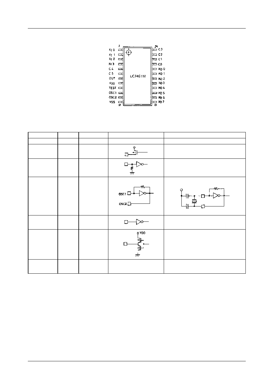
Pin Assignment
Top view
Pin Description
Pin Name
Pin No.
Input/Output
Internal Equivalent Circuit
Pin Function
V
DD
, V
SS
8, 12
Power supply pins V
SS
= GND
K
O
0 to K
O
7
13 to 20
Output
Key scan timing signal output pins
K
I
0 to K
I
3
1 to 4
Input
Keys return signal entry pins
OSC1
OSC2
10
11
Input/output
Input/output pins for ceramic resonator-used
oscillation
Oscillator configuration
C
0
to C
5
21 to 24,
5, 6
Input
Input pins for custom code setting
Capable of externally setting 6 bits of 13 bits in
all that provide a custom code
OUT
7
Output
Output pin for transmit LED drive
TEST
9
Input
LSI test pin
Normally set to high-level or brought to open
state
LC7461M
No.2119-3/7

General Description of Function
1.
Oscillator
Since a self-bias type amplifier of CMOS inverter is contained, an oscillator can be formed by connecting a ceramic
resonator.
To minimize power dissipation, the oscillator stops oscillating except when key operation is performed.
2.
Key entry
Key entry pins K
I
0 to K
I
3 and timing signal output pins K
O
0 to K
O
7 provide a key matrix of 4
◊
8 = 32.
Multi-press of key No. 20 and one of key No. 21, 22, 23 may be done, with no priority given in key entry. When the two
keys are kept pressed, a series of pulses will be output according to each key entry. If multi-press of keys which are not
allowed multi-press is done, no output will be delivered.
3.
Data organization
Data consists of 42 bits in all: 13 bits of custom code, 8 bits of key data, and their inverted codes.
Custom code
Custom code
Key data
Key data
13 bits
13 bits
8 bits
8 bits
LC7461M
No.2119-4/7
(a) Custom code
The custom code, which consists of 13 bits (C
0
to C
12
) in all, is used to distinguish between receiving sets.
C
6
to C
12
are fixed by the mask ROM and C
0
to C
5
are pin-settable.
The custom codes are controlled by Sanyo to avoid duplication.
(b) Key data
When multi-press of key No.20 and one of key No.21, 22, 23 is done, multi-bit D
5
will be set to ``1'', with no priority given
in key entry.
Pin-selectable
Mask ROM
6 bits
7 bits
In this example C
0
to C
5
are
set as follows:
C
0
C
1
C
2
C
3
C
4
C
5
0
1
1
0
0
1
Multi-press
KEY No.
D
0
D
1
D
2
D
3
D
4
D
5
D
6
D
7
20, 21
1
0
1
0
1
1
0
0
20, 22
0
1
1
0
1
1
0
0
20, 23
1
1
1
0
1
1
0
0
.
D
6
, D
7
may be preset to ``0'',``1'' beforehand (mask
option).
KEY No.
D
0
D
1
D
2
D
3
D
4
D
5
D
6
D
7
0
0
0
0
0
0
0
0
0
1
1
0
0
0
0
0
0
0
2
0
1
0
0
0
0
0
0
3
1
1
0
0
0
0
0
0
4
0
0
1
0
0
0
0
0
5
.
.
.
28
1
.
.
.
0
0
.
.
.
0
1
.
.
.
1
0
.
.
.
1
0
.
.
.
1
0
.
.
.
0
0
.
.
.
0
0
.
.
.
0
29
1
0
1
1
1
0
0
0
30
0
1
1
1
1
0
0
0
31
1
1
1
1
1
0
0
0
(H: Key-ON state)
Key 20
data
transmit
Keys 20, 21
multi-press
data transmit
Key 21
data
transmit
Transmit
stop
Key 22
data
transmit
Keys 20, 22
multi-press data
transmit
LC7461M
No.2119-5/7
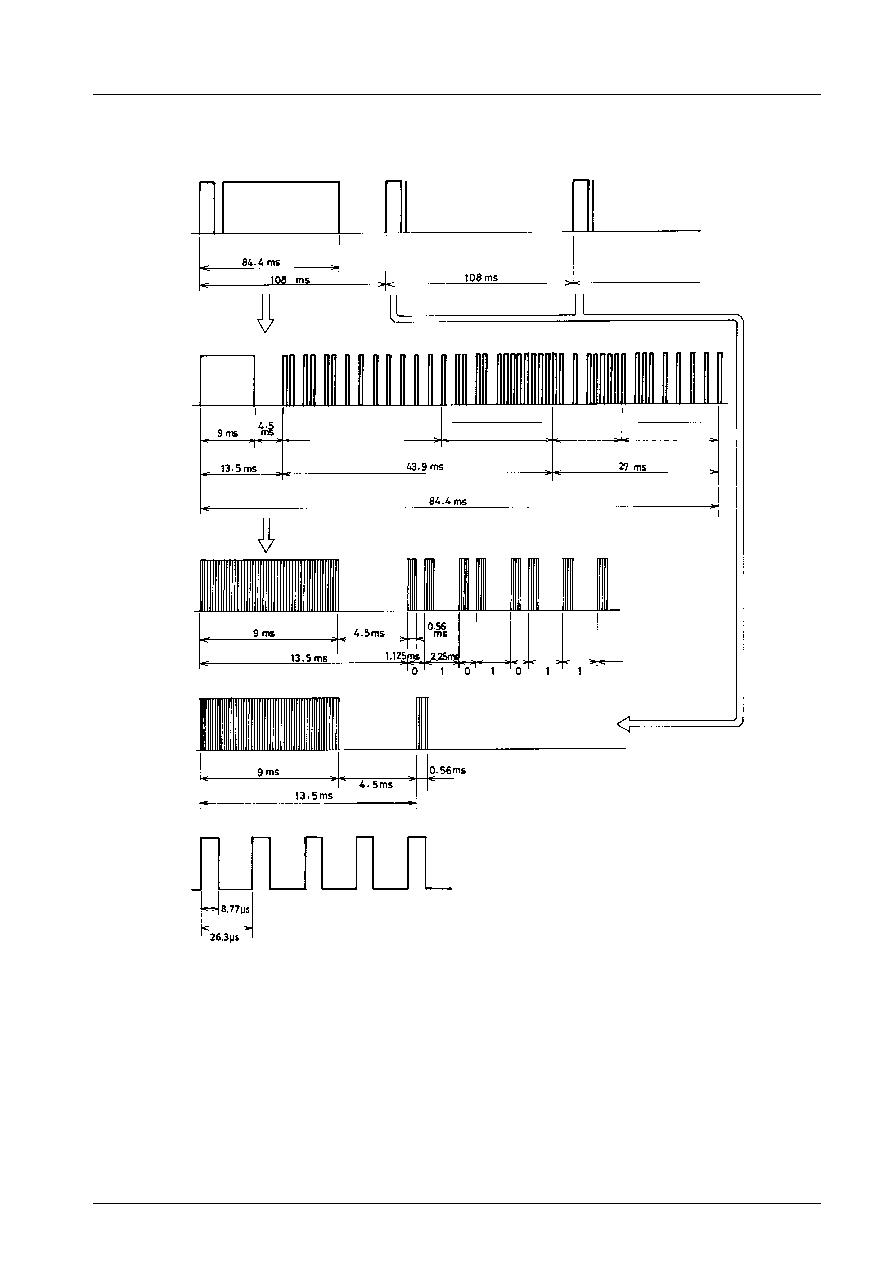
4.
Transmit waveforms
The period of time shown below is for f
OSC
= 455 kHz.
Custom code
Custom code
Key data
Key data
13 bits
13 bits
8 bits
8 bits
Leader code
.
First time
.
Second time onward (Transmission is available only when key entry continues.)
.
Carrier waveform
Carrier frequency = 1/12 f
OSC
7
38 kHz
LC7461M
No.2119-6/7

Sample Application Circuit
In this example custom code C
0
to C
5
is C
0
z z z z z
C
5
.
0 1 0 1 0 1
No products described or contained herein are intended for use in surgical implants, life-support systems, aerospace equipment,
nuclear power control systems, vehicles, disaster/crime-prevention equipment and the like, the failure of which may directly or
indirectly cause injury, death or property loss.
Anyone purchasing any products described or contained herein for an above-mentioned use shall:
1
Accept full responsibility and indemnify and defend SANYO ELECTRIC CO., LTD., its affiliates, subsidiaries and distributors
and all their officers and employees, jointly and severally, against any and all claims and litigation and all damages, cost and
expenses associated with such use:
2
Not impose any responsibility for any fault or negligence which may be cited in any such claim or litigation on SANYO
ELECTRIC CO., LTD., its affiliates, subsidiaries and distributors or any of their officers and employees jointly or severally.
Information (including circuit diagrams and circuit parameters) herein is for example only; it is not guaranteed for volume
production. SANYO believes information herein is accurate and reliable, but no guarantees are made or implied regarding its use
or any infringements of intellectual property rights or other rights of third parties.
This catalog provides information as of October, 1996. Specifications and information herein are subject to change without notice.
Transmit
LED
LC7461M
No.2119-7/7