 | –≠–ª–µ–∫—Ç—Ä–æ–Ω–Ω—ã–π –∫–æ–º–ø–æ–Ω–µ–Ω—Ç: LC74770M | –°–∫–∞—á–∞—Ç—å:  PDF PDF  ZIP ZIP |
Ordering number : EN4248A
31596HA (OT) No. 4248-1/11
Overview
The LC74770M is a CMOS LSI that implements on-
screen display, a function that displays characters and
patterns on display screens such as camcorder viewfinder
screens under microprocessor control. This LSI displays
12-dot by 18-dot characters.
Features
∑ Display format: 24 characters by 12 rows (up to
288 characters)
∑ Characters displayed: Up to 288 characters
∑ Character format: 12 (horizontal)
◊
18 (vertical)
∑ Characters in font: 128
∑ Character sizes: Normal and double
∑ Initial display positions: 64 horizontal positions and
64 vertical positions
∑ Reverse video function: Characters can be displayed in
reverse video specified in units of individual characters.
∑ Blinking types: In character units in one of two periods,
1.0 second and 0.5 second, with a 50% duty.
∑ Outputs: Character and blanking data, with two output
systems for each
∑ External control input: 8-bit serial input format
∑ General-purpose output port: 4 bits (controlled from the
serial input data)
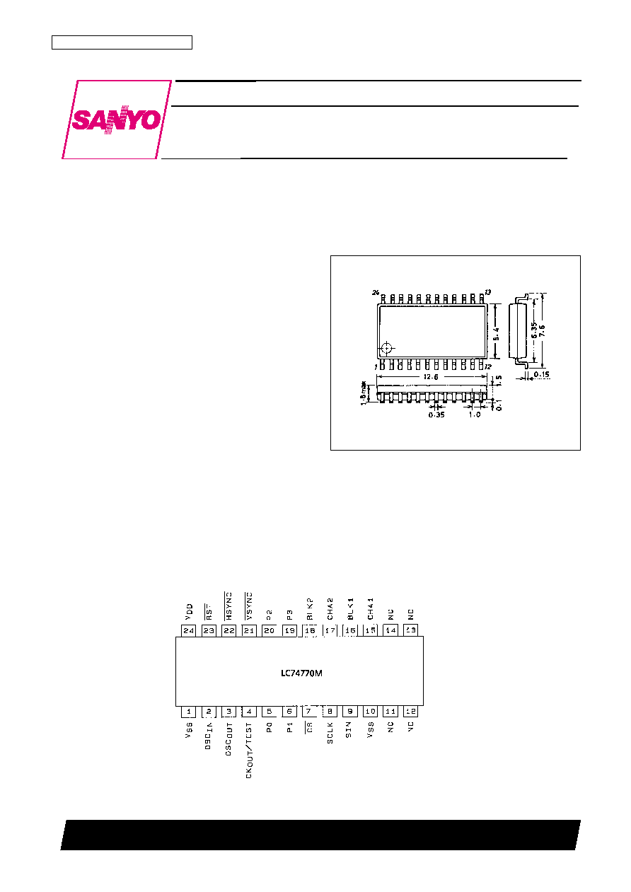
Pin Assignment
Package Dimensions
unit: mm
3112-MFP24S
SANYO: MFP24S
[LC74770M]
LC74770M
SANYO Electric Co.,Ltd. Semiconductor Bussiness Headquarters
TOKYO OFFICE Tokyo Bldg., 1-10, 1 Chome, Ueno, Taito-ku, TOKYO, 110-0005 JAPAN
On-Screen Display Controller LSI
CMOS LSI
Top view
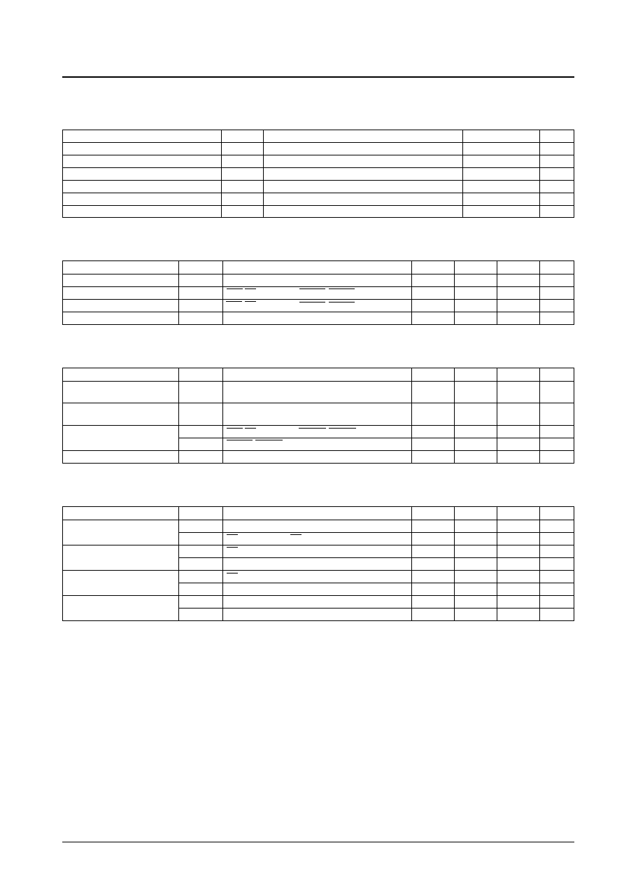
Specifications
Absolute Maximum Ratings
at Ta = 25∞C
Allowable Operating Ranges
at Ta = ≠30 to +70∞C
Electrical Characteristics
at Ta = ≠30 to +70∞C, V
DD
= 5 V unless otherwise specified.
Timing Characteristics
at Ta = ≠30 to +70∞C, V
DD
= 5 ± 0.5 V
No. 4248-2/11
LC74770M
Parameter
Symbol
Conditions
Ratings
Unit
Maximum supply voltage
V
DD
max
V
DD
V
SS
≠ 0.3 to V
SS
+ 7.0
V
Maximum input voltage
V
IN
max
All input pins
V
SS
≠ 0.3 to V
DD
+ 0.3
V
Maximum output voltage
V
OUT
max
BLK1, BLK2, CHA1, CHA2, P0 to P3, CK
OUT
V
SS
≠ 0.3 to V
DD
+ 0.3
V
Allowable power dissipation
Pd max
300
mW
Operating temperature
Topr
≠30 to +70
∞C
Storage temperature
Tstg
≠40 to +125
∞C
Parameter
Symbol
Conditions
min
typ
max
Unit
Supply voltage
V
DD
V
DD
4.5
5.0
5.5
V
Input high-level voltage
V
IH
RST, CS, SIN, SCLK, HSYNC, VSYNC
0.8 V
DD
V
DD
+ 0.3
V
Input low-level voltage
V
IL
RST, CS, SIN, SCLK, HSYNC, VSYNC
V
SS
≠ 0.3
0.2 V
DD
V
Oscillator frequency
f
OSC
OSC
IN
and OSC
OUT
oscillator pins
5
7
10
MHz
Parameter
Symbol
Conditions
min
typ
max
Unit
Output high-level voltage
V
OH
BLK1, BLK2, CHA1, CHA2, P0 to P3: V
DD
= 5.0 V,
4.5
V
I
OH
= ≠1.0 mA
Output low-level voltage
V
OL
BLK1, BLK2, CHA1, CHA2, P0 to P3: V
DD
= 5.0 V,
0.5
V
I
OL
= 1.0 mA
Input current
I
IH
RST, CS, SIN, SCLK, HSYNC, VSYNC: V
IN
= V
DD
1
µA
I
IL
HSYNC, VSYNC: V
IN
= V
SS
≠1
µA
Operating current drain
I
DD
V
DD
: all outputs open, LC = 7 MHz
10
mA
Parameter
Symbol
Conditions
min
typ
max
Unit
Minimum input pulse width
t
W (SCLK)
SCLK
200
ns
t
W (CS)
CS (the period that CS is high)
1
µs
Data setup time
t
SU (CS)
CS
200
ns
t
SU (SIN)
SIN
200
ns
Data hold time
t
h (CS)
CS
2
µs
t
h (SIN)
SIN
200
ns
Single word write time
t
word
The time to write 8 bits of data
4.2
µs
t
wt
The time to write RAM data
1
µs
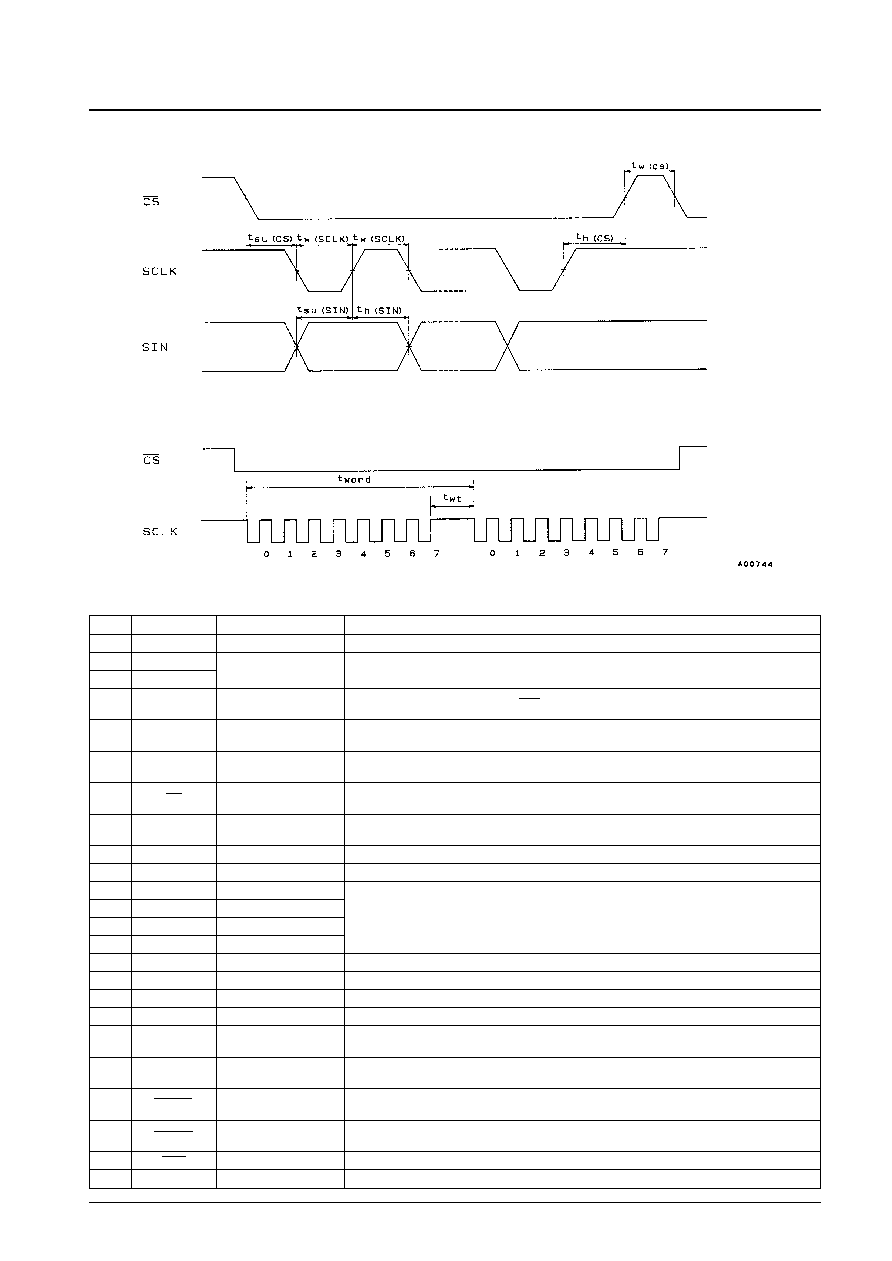
Serial Data Input Timing
Pin Functions
No. 4248-3/11
LC74770M
No.
Symbol
Pin
Function
1
V
SS
Ground pin
Ground connection
2
OSC
IN
LC oscillator pin
Connections for the coil and capacitor that form the oscillator that generates the character output
3
OSC
OUT
dot clock.
4
CK
OUT
/TEST
Clock output/test
Provides the OSC
OUT
output (when RST is low) and the test mode output.
output pin
5
P0
General-purpose port 0
General-purpose port (PORT0) output
output pin
6
P1
General-purpose port 1
General-purpose port (PORT1) output
output pin
7
CS
Enable input pin
Enable input for the serial data input function. Serial data input is enabled when this pin is low.
A pull-up resistor is built in, i.e., this is a hysteresis input.
8
SCLK
Clock input pin
Clock input for the serial data input function. A pull-up resistor is built in,
i.e., this is a hysteresis input.
9
SIN
Data input pin
Serial data input. A pull-up resistor is built in, i.e., this is a hysteresis input.
10
V
SS
Ground pin
Ground connection
11
NC
No connection
12
NC
No connection
Unused pins.
13
NC
No connection
These pins must be left open or connected to ground.
14
NC
No connection
15
CHA1
Character 1 output pin
System 1 character data output
16
BLK1
Blank 1 output pin
System 1 blank data output
17
CHA2
Character 2 output pin
System 2 character data output
18
BLK2
Blank 2 output pin
System 2 blank data output
19
P3
General-purpose port 3
General-purpose port (PORT3) output
output pin
20
P2
General-purpose port 2
General-purpose port (PORT2) output
output pin
21
VSYNC
Vertical synchronizing
Input for the vertical synchronizing signal (active low)
signal input pin
22
HSYNC
Horizontal synchronizing
Input for the horizontal synchronizing signal (active low)
signal input pin
23
RST
Reset input pin
System reset input (active low) A pull-up resistor is built in, i.e., this is a hysteresis input.
24
V
DD
Power supply pin (+5 V)
Power supply (+5 V)
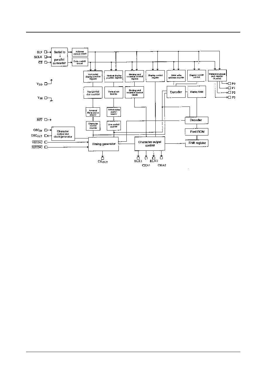
Block Diagram
Display Control Commands
Display control commands have an 8-bit format and are transferred using the serial input function. Commands consist of
a command identification code in the first byte and command data in the following bytes. The following commands are
supported.
1 COMMAND 0: Display memory (VRAM) write address setup command
2 COMMAND 1: Display character data write command
3 COMMAND 2: Vertical display start position and vertical character size setup command
4 COMMAND 3: Horizontal display start position and horizontal character size setup command
5 COMMAND 4: Display control setup command
6 COMMAND 5: System 2 (BLK2 and CHA2) output control (lines 1 to 6) and line size setting command
7 COMMAND 6: System 2 (BLK2 and CHA2) output control (lines 7 to 12) and general-purpose port setting command
No. 4248-4/11
LC74770M
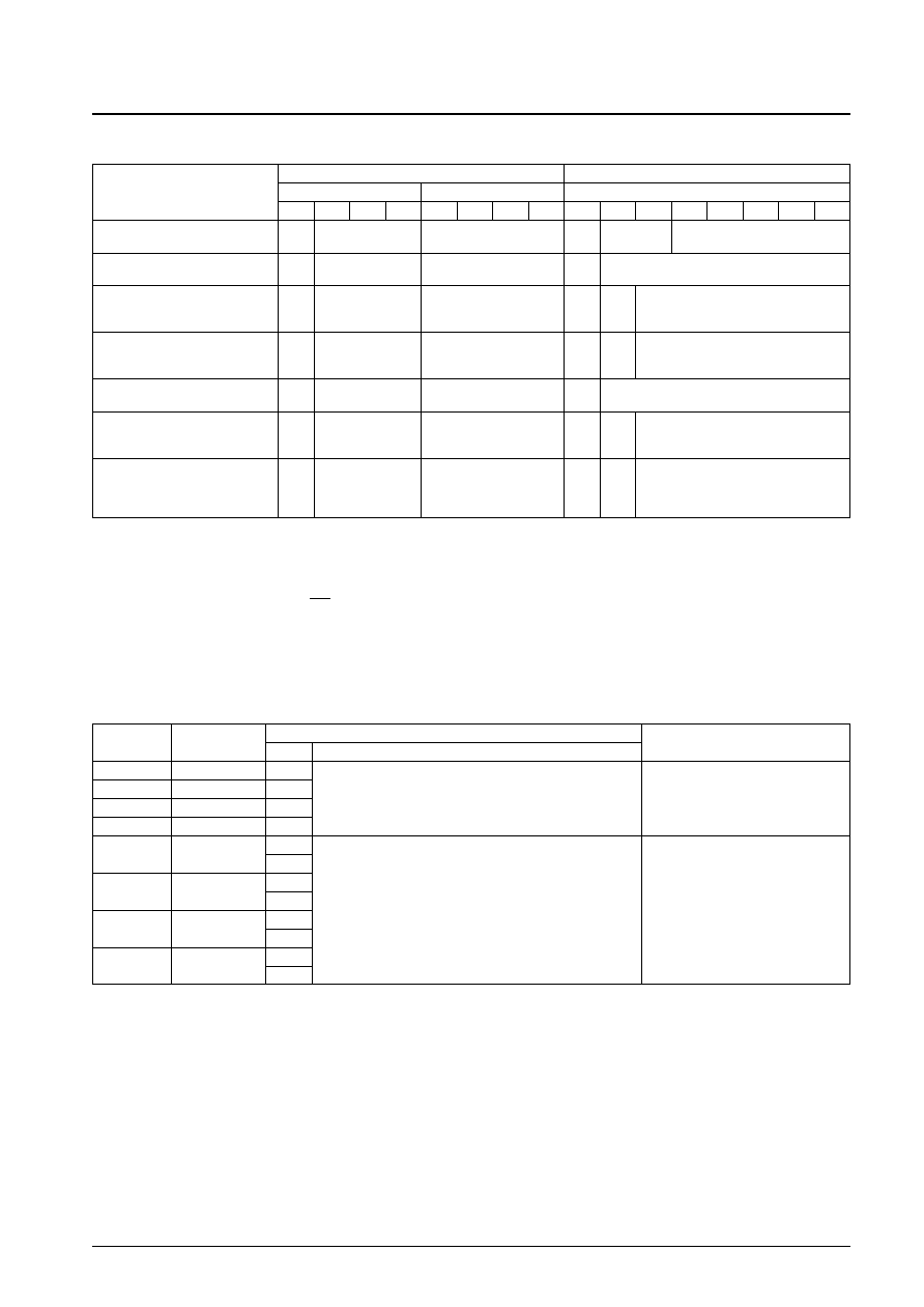
Display Control Command Table
Once written, the command identification code in the first byte is stored until the next first byte is written. However,
when the display character data write command (COMMAND1) is written, the LC74770M locks into the display
character data write mode, and another first byte cannot be written.
When a high level is input to the CS pin, the LC74770M is set to COMMAND0 (display memory write address setup
mode).
1
COMMAND 0 (Display memory write address setup command)
First byte
No. 4248-5/11
LC74770M
First byte
Second byte
Command
Command identification code
Data
Data
7
6
5
4
3
2
1
0
7
6
5
4
3
2
1
0
COMMAND 0
1
0
0
0
V3
V2
V1
V0
0
0
0
H4
H3
H2
H1
H0
Write address
COMMAND 1
1
0
0
1
0
0
0
0
at
c6
c5
c4
c3
c2
c1
c0
Character write
COMMAND 2
1
0
1
0
0
0
0
0
0
0
VP
VP
VP
VP
VP
VP
Vertical display position
5
4
3
2
1
0
start position
COMMAND 3
1
0
1
1
0
0
0
0
0
0
HP
HP
HP
HP
HP
HP
Horizontal display position
5
4
3
2
1
0
start position
COMMAND 4
1
1
0
0
TST
RCL
OSC
RST
0
MD1
MD0
EG
BK
BK
RV
DSP
Display control
1
0
COMMAND 5
1
1
0
1
0
0
0
LS
0
0
LN
LN
LN
LN
LN
LN
BLK2 and CHA2 output control:
6
5
4
3
2
1
lines 1 to 6, and line size control
COMMAND 6
BLK2 and CHA2 output control:
1
1
1
0
P3
P2
P1
P0
0
0
LN
LN
LN
LN
LN
LN
lines 7 to 12, and general-purpose
12
11
10
9
8
7
port control
Register content
DA0 to DA7
Register name
State
Function
Note
7
--
1
6
--
0
Command 0 identification code
5
--
0
Sets the display memory write address.
4
--
0
3
V3
0
1
2
V2
0
1
Display memory address (0 to B hexadecimal)
1
V1
0
1
0
V0
0
1