 | –≠–ª–µ–∫—Ç—Ä–æ–Ω–Ω—ã–π –∫–æ–º–ø–æ–Ω–µ–Ω—Ç: LC74772V | –°–∫–∞—á–∞—Ç—å:  PDF PDF  ZIP ZIP |
Overview
The LC74772V is a CMOS LSI that implements on-screen
display for camcorders. It displays characters and patterns
in a camcorder viewfinder under microprocessor control.
The LC74772V displays a 12
◊
18 dot font with 256
characters.
Features
∑ Screen format: 12 lines • 24 characters (up to 288
characters)
∑ Number of characters displayed: Up to 288 characters
∑ Character format: 12 (horizontal)
◊
18 (vertical) dots
∑ Number of characters in font: 256 characters
∑ Character sizes: Normal and double, specified in line
units
∑ Display start position
-- Horizontal: 64 positions
-- Vertical: 64 positions
∑ Character reverse video function: Individual characters
can be displayed in reverse video.
∑ Types of blinking: Two types with periods of 1.0 and
0.5 seconds, specifiable on a per character basis.
(Blinking has a 60% display on duty.)
(Four divisors: 1/25, 1/30, 1/50, 1/60)
∑ Outputs: R, G, B plus 2 output systems
Or: 4 output systems (character data and blanking data:
4 outputs each)
∑ External control input: 8-bit serial data input format
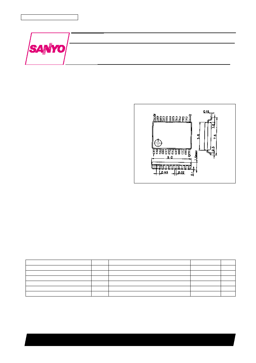
Package Dimensions
unit: mm
3175A-SSOP24
CMOS LSI
O3096HA(OT)/D3095HA (OT) No. 5159-1/16
SANYO: SSOP24
[LC74772V]
SANYO Electric Co.,Ltd. Semiconductor Bussiness Headquarters
TOKYO OFFICE Tokyo Bldg., 1-10, 1 Chome, Ueno, Taito-ku, TOKYO, 110 JAPAN
Camcorder On-Screen Display LSI
LC74772V
Ordering number : EN5159A
Parameter
Symbol
Conditions
Ratings
Unit
Supply voltage
V
DD
V
DD
V
SS
≠ 0.3 to V
SS
+ 7.0
V
Input voltage
V
IN
All input pins
V
SS
≠ 0.3 to V
DD
+ 0.3
V
Output voltage
V
OUT
CK
OUT
, CHA4, BLK4, CHA3, BLK3, B, G, R, BLANK
V
SS
≠ 0.3 to V
DD
+ 0.3
V
Allowable power dissipation
Pd max
Ta = 25∞C
300
mW
Operating temperature
Topr
≠30 to +70
∞C
Storage temperature
Tstg
≠40 to +125
∞C
Specifications
Absolute Maximum Ratings

No. 5159-2/16
LC74772V
Parameter
Symbol
Conditions
Ratings
Unit
min
typ
max
Supply voltage
V
DD
V
DD
2.7
5.0
5.5
V
Input high-level voltage
V
IH
CTRL1, TEST
IN
, CS, SCLK, SIN, OUT
MOD
, HSYNC,
0.8 V
DD
V
DD
+ 0.3
V
VSYNC, RST
Input low-level voltage
V
IL
CTRL1, TEST
IN
, CS, SCLK, SIN, OUT
MOD
, HSYNC,
V
SS
≠ 0.3
0.2 V
DD
V
VSYNC, RST
Oscillator frequency
F
OSC
OSC
IN
, OSC
OUT
(LC oscillator)
6
(8)
10
MHz
Allowable Operating Ranges
at Ta = ≠30 to +70∞C
Parameter
Symbol
Conditions
Ratings
Unit
min
typ
max
CK
OUT
, CHA4, BLK4, CHA3, BLK3, B, G, R, BLANK:
Output high-level voltage
V
OH
V
DD
= 5.5 to 4.5 V (V
DD
= 4.4 to 2.7 V), I
OH
= ≠1.0 mA
0.9 V
DD
V
(≠0.5 mA)
CK
OUT
, CHA4, BLK4, CHA3, BLK3, B, G, R, BLANK:
Output low-level voltage
V
OL
V
DD
= 5.5 to 4.5 V (V
DD
= 4.4 to 2.7 V), I
OL
= 1.0 mA
0.1 V
DD
V
(0.5 mA)
I
IH
CTRL1, TEST
IN
, CS, SCLK, SIN, OUT
MOD
, HSYNC,
1
µA
Input current
VSYNC: V
IN
= V
DD
I
IL
CTRL1, TEST
IN
, HSYNC, VSYNC: V
IN
= V
SS
≠1
µA
Operating current drain
I
DD
V
DD
pin; all outputs open, LC oscillator: 8 MHz
10
mA
Electrical Characteristics
at Ta = ≠30 to +70∞C, unless otherwise specified V
DD
= 5 V
Parameter
Symbol
Conditions
Ratings
Unit
min
typ
max
Minimum input pulse width
t
W (SCLK)
SCLK
200
ns
t
W (CS)
CS (the period that CS is high)
1
µs
Data setup time
t
SU (CS)
CS
200
ns
t
SU (SIN)
SIN
200
ns
Data hold time
t
h (CS)
CS
2
µs
t
h (SIN)
SIN
200
ns
One-word write time
t
word
The time to write 8 bits of data
4.2
µs
t
wt
The RAM data write time
1
µs
Timing Characteristics
at Ta = ≠30 to +70∞C, V
DD
= 5 ± 0.5 V
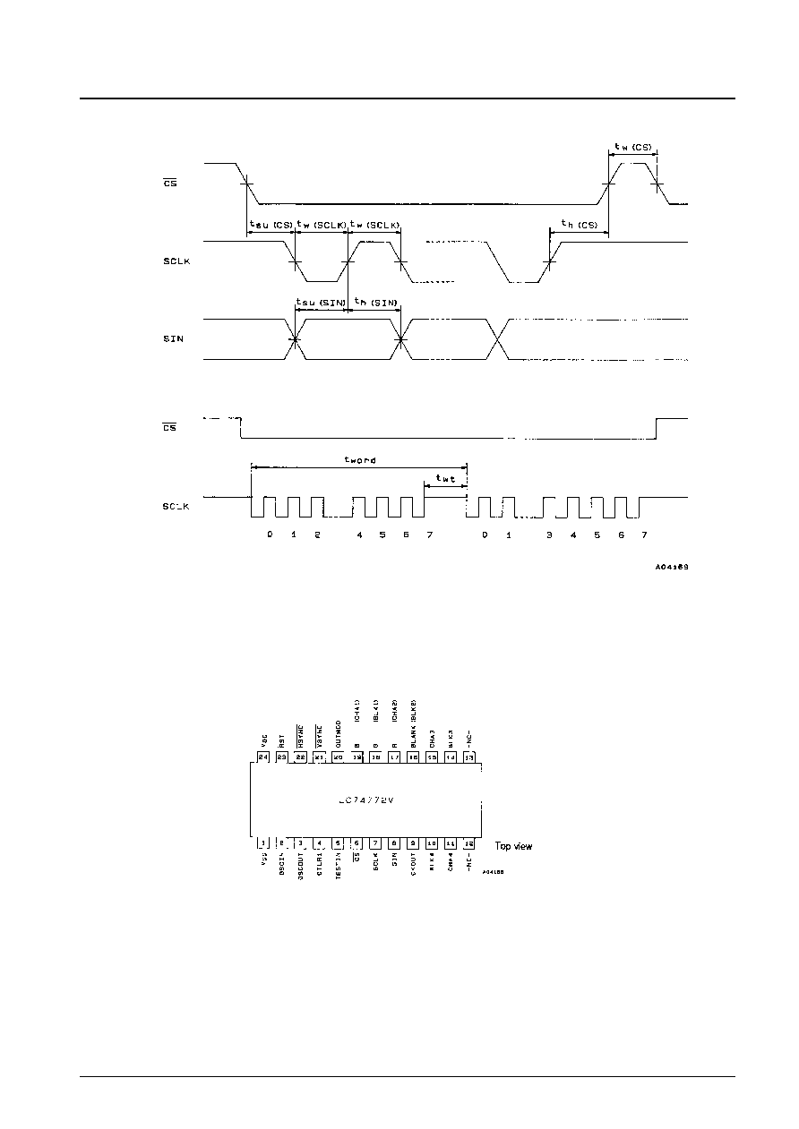
Serial Data Input Timing
Pin Assignment
The signal names in parentheses indicate the output pin functions when 4-system output mode is used.
No. 5159-3/16
LC74772V
No. 5159-4/16
LC74772V
Pin Functions
PinNo.
Symbol
Function
Description
1
V
SS
Ground
Ground connection
2
OSC
IN
LC oscillator
Connections for the coil and capacitor that form the oscillator that generates the character
3
OSC
OUT
output horizontal dot clock.
4
CTRL1
Clock input control
Control input that switches between LC oscillator mode and clock input mode
Low: LC oscillator mode, high: clock input mode
5
TEST
IN
Test control input
Test mode control input (The IC operates in test mode when this input is high.)
6
CS
Enable input
Serial data input enable input
Low: active (This input has hysteresis characteristics.)
7
SCLK
Clock input
Serial data input clock input (This input has hysteresis characteristics.)
8
SIN
Data input
Serial data input (This input has hysteresis characteristics.)
9
CK
OUT
Clock output
LC oscillator clock monitor output
This signal is output when RST is low.
10
BLK4
Blanking signal output
Blanking signal output (system 2)
Functions as the system 4 blanking data signal output in 4-system mode.
11
CHA4
Character data output
Character data signal output (system 2)
Functions as the system 4 character data signal output in 4-system mode.
12
NC
Unused
Must be left open or tied to ground in normal operation.
13
NC
Unused
Must be left open or tied to ground in normal operation.
14
BLK3
Blanking signal output
Blanking signal output (system 1)
Functions as the system 3 blanking data signal output in 4-system mode.
15
CHA3
Character data output
Character data signal output (system 1)
Functions as the system 3 character data signal output in 4-system mode.
16
BLANK
Blanking signal output
Blanking signal output (blanking signal for RGB output)
Functions as the system 2 blanking data signal output in 4-system mode.
17
R
Character data output
Character data (R) signal output
Functions as the system 2 character data signal output in 4-system mode.
18
G
Character data output
Character data (G) signal output
Functions as the system 1 blanking data signal output in 4-system mode.
19
B
Character data output
Character data (B) signal output
Functions as the system 1 character data signal output in 4-system mode.
20
OUT
MOD
Output control input
Control input that switches between RGB output and 4-system output
Low: RGB output, high 4-system output
21
VSYNC
Vertical synchronizing
Vertical synchronizing signal input (This input has hysteresis characteristics.)
signal input
22
HSYNC
Horizontal synchronizing
Horizontal synchronizing signal input (This input has hysteresis characteristics.)
signal input
23
RST
Reset input
System reset signal input (This input has hysteresis characteristics.)
24
V
DD
Power supply
Power supply connection (+5 V)
Note: 1. Built-in pull-up resistors can be specified for inclusion in the CS (pin 6), SCLK (pin 7), SIN (pin 8), and RST (pin 23) pins as mask options.
2. In clock input mode (when CTRL1 is high), the function that holds the OSC
IN
(pin 2) pin high during an oscillator reset is stopped.
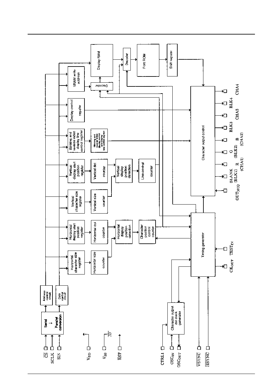
Block Diagram
No. 5159-5/16
LC74772V