 | –≠–ª–µ–∫—Ç—Ä–æ–Ω–Ω—ã–π –∫–æ–º–ø–æ–Ω–µ–Ω—Ç: LC74776 | –°–∫–∞—á–∞—Ç—å:  PDF PDF  ZIP ZIP |
Overview
The LC74776/M is an on-screen display controller CMOS
IC that displays characters and patterns on the TV screen
under microprocessor control. This IC includes a built-in
PDC/VPS/UDT interface circuit.
Functions
∑ Display format: 24 characters by 12 rows (Up to 288
characters)
∑ Character format: 12 (horizontal)
◊
18 (vertical) dots
∑ Character sizes: Three sizes each in the horizontal and
vertical directions
∑ Characters in font: 256 (Of the 256 characters, one is a
space character (FE hexadecimal)
and one is a transparent space
character (FF hexadecimal))
∑ Initial display positions: 64 horizontal positions and 64
vertical positions
∑ Blinking: Specifiable in character units
∑ Blinking types: Two periods supported:
1.0 second and 0.5 second
∑ Blanking: Over the whole font (12
◊
18 dots)
∑ Background color: 8 colors (internal synchronization
mode): 4f
SC
and 2f
SC
Blue background only: NTSC
∑ Line background color: Three lines can be set up.
8 line background colors (in
internal synchronization mode):
4f
SC
and 2f
SC
∑ External control input: 8-bit serial input format
∑ On-chip sync separator circuit
∑ Video outputs: PAL and NTSC format composite video
outputs
∑ On-chip PDC/VPS/UDT interface circuit supporting I
2
C
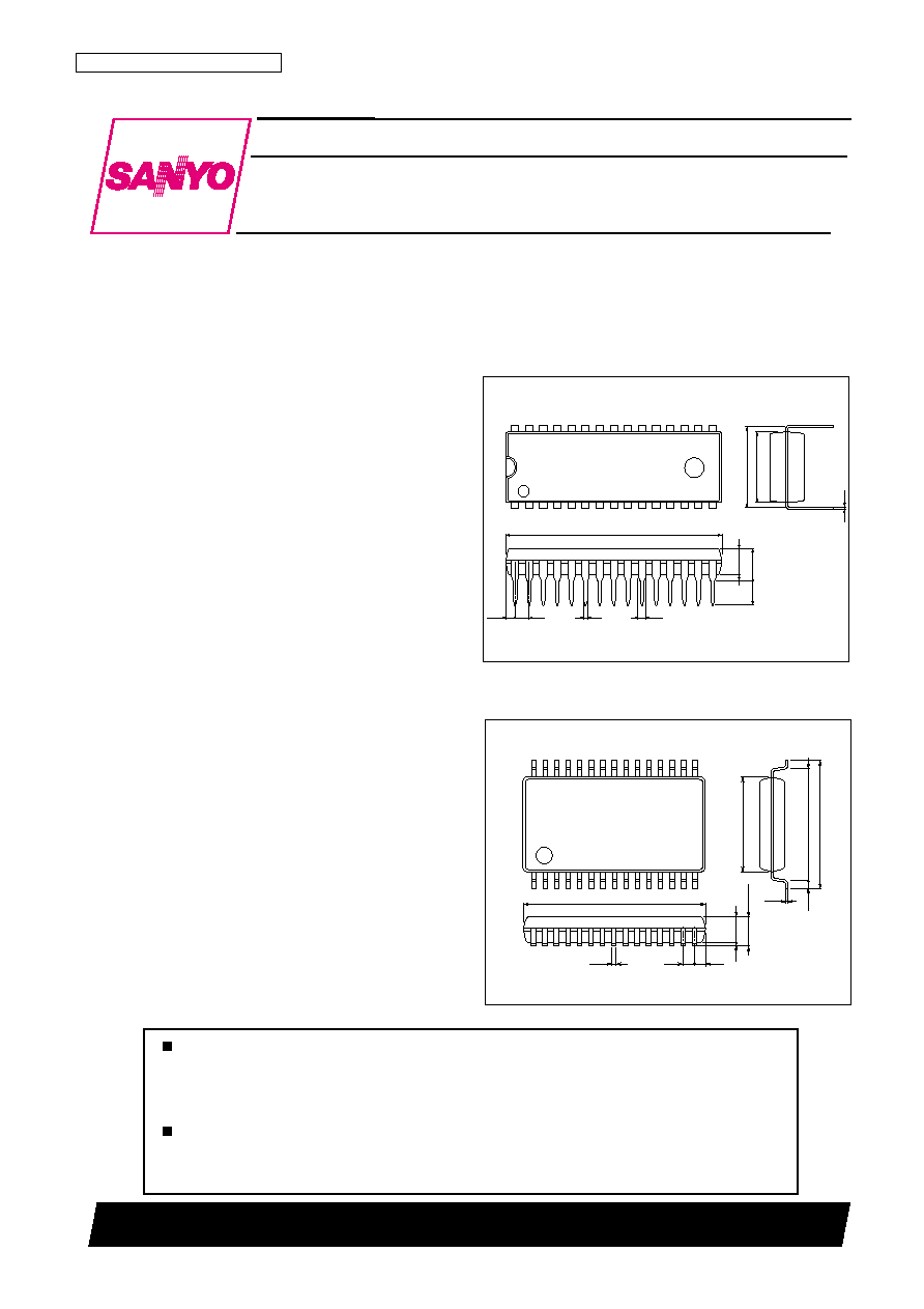
∑ Package: DIP30SD
MFP30S
0.15
15.3
1
15
30
16
0.65
1.0
0.35
2.5max
2.15
0.1
0.65
7.9
9.2
10.5
CMOS IC
Ordering number : EN
*
6018
20399RM(OT) No. 6018-1/35
Preliminary
SANYO: MFP30S
[LC74776M]
SANYO Electric Co.,Ltd. Semiconductor Bussiness Headquarters
TOKYO OFFICE Tokyo Bldg., 1-10, 1 Chome, Ueno, Taito-ku, TOKYO, 110-8534 JAPAN
On-Screen Display Controller IC
LC74776, 74776M
1
15
30
16
1.14
1.78
27.2
0.25
10.16
8.6
0.48
0.95
3.25
3.0
3.95max
SANYO: DIP30SD
[LC74776]
Package Dimensions
unit: mm
3196-DIP30SD
unit: mm
3216A-MFP30S
Any and all SANYO products described or contained herein do not have specifications that can handle
applications that require extremely high levels of reliability, such as life-support systems, aircraft's
control systems, or other applications whose failure can be reasonably expected to result in serious
physical and/or material damage. Consult with your SANYO representative nearest you before using
any SANYO products described or contained herein in such applications.
SANYO assumes no responsibility for equipment failures that result from using products at values that
exceed, even momentarily, rated values (such as maximum ratings, operating condition ranges, or other
parameters) listed in products specifications of any and all SANYO products described or contained
herein.
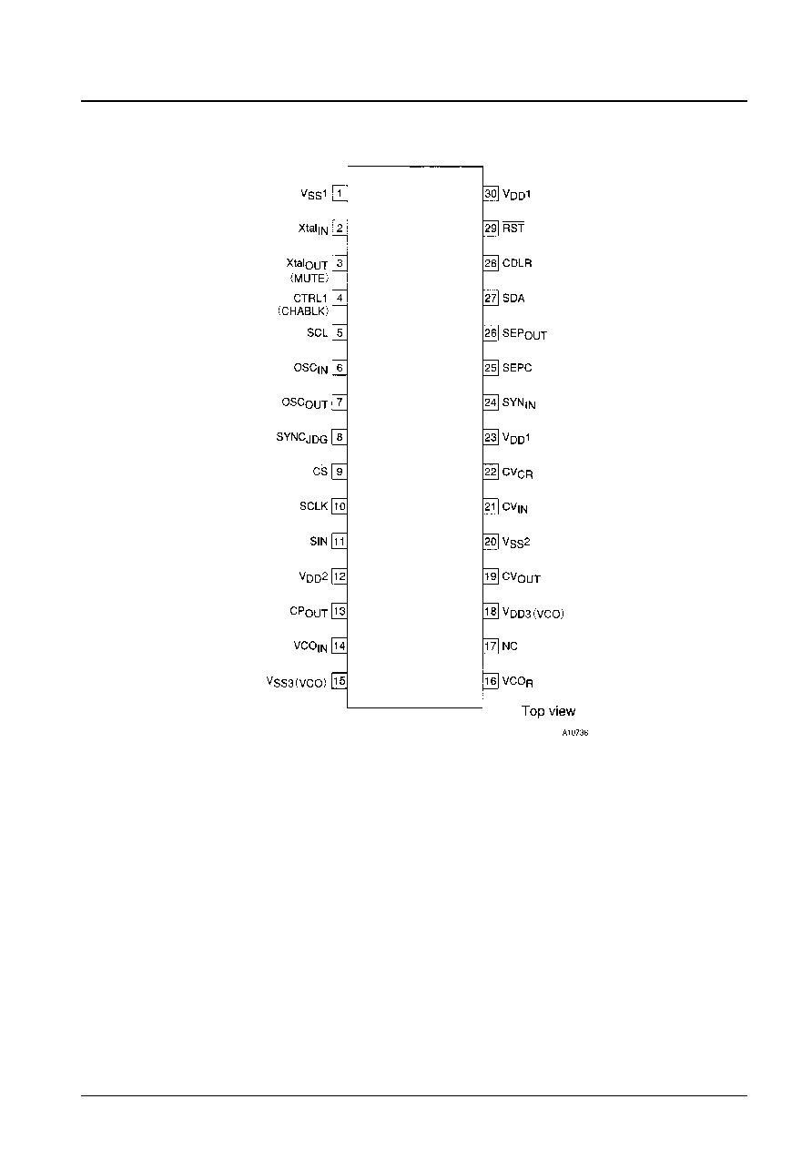
Pin Assignment
No. 6018-2/35
LC74776, 74776M
LC74776
LC74776M
Pin Functions
No. 6018-3/35
LC74776, 74776M
Pin no.
Pin
Function
Notes
1
V
SS
1
Ground
Ground connection (digital system ground)
2
Xtal
IN
These pins are used either to connect the crystal and capacitors used to form an external
crystal oscillator circuit to generate the internal synchronizing signals, or to input an external
Xtal
OUT
Crystal oscillator
clock signal (2fsc or 4fsc). As a mask option, the Xtal
OUT
pin can be set to function as
3
(MUTE)
(MUTE input)
the MUTE input pin. When this pin is set low, the video output is held at the pedestal level.
(A pull-up resistor is built in and the input has hysteresis characteristics.)
Switches the mode between external clock input and crystal oscillator operation. A low level
4
CTRL1
selects crystal oscillator operation and a high level selects external clock input. As a mask
(CHABLK)
option, the CTRL1 input pin can be set to function as the CHABLK (character
.
frame)
output. This is a 3-value output.
5
SCL
I
2
C clock input
Clock input for the PDC/VPS data output. I
2
C bus.
6
OSC
IN
LC oscillator
Connection for the external coil and capacitor for the oscillator used to generate
connections
the character output dot clock
7
OSC
OUT
Outputs the state of the external synchronizing signal presence/absence judgment. Outputs
External synchronizing
a high level when synchronizing signals are present.
8
SYNC
JDC
signal judgment output
Outputs either the crystal oscillator clock if CS and RST are low, or the VCO clock if CS
and RST are high.
(This signal is not output after a command reset.)
Enable input for the OSD serial data input.
9
CS
Enable input
Serial data input is enabled when this pin is low.
A pull-up resistor is built in and the input has hysteresis characteristics.
10
SCLK
Clock input
Serial data input enable pin.
A pull-up resistor is built in and the input has hysteresis characteristics.
11
SIN
Data input
Serial data input.
A pull-up resistor is built in and the input has hysteresis characteristics.
12
V
DD
2
Power supply
Composite video signal level adjustment power supply (analog system power supply)
13
CP
OUT
Charge pump output
Charge pump output. Connect a low-pass filter to this pin.
14
VCO
IN
Oscillator control voltage input
VCO oscillator control voltage input. (For data slicing)
15
V
SS
3
Ground
Ground (VCO ground)
16
VCO
R
Oscillator range adjustment
VCO oscillator range adjustment resistor connection
17
NC
This pin must either be connected to ground or left open
18
V
DD
3
Power supply (+5 V)
Power supply (+5 V: VCO power supply)
19
CV
OUT
Video signal output
Composite video signal output
20
V
SS
2
Ground
Ground (analog system ground)
21
CV
IN
Video signal input
Composite video signal input
22
CV
CR
Video signal input
SECAM chrominance signal input
23
V
DD
1
Power supply (+5 V)
Power supply (+5 V: digital system power supply)
24
SYN
IN
Sync separator circuit input
Video signal input to the internal sync separator circuit
25
SEPC
Slice level output
Slice level verification pin
26
SEP
OUT
Composite synchronizing
Internal sync separator circuit composite synchronizing signal output. The signal actually
signal output
output can be switched by MOD0 and SEL0. The DAV signal is output in the initial state.
PDC/VPS data I/O.
27
SDA
I
2
C bus data I/O
The I
2
C bus write address is [0111 1100].
The I
2
C bus read address is [0111 1101].
28
CDLR
Background color phase
Background color phase adjustment resistor connection
adjustment
29
RST
Reset input
System reset input.
A pull-up resistor is built in and the input has hysteresis characteristics.
30
V
DD
1
Power supply (+5 V)
Power supply (+5 V: digital system power supply)
Note:
*
Both V
DD
1 pins must be connected to power.
Crystal oscillator input
switching
(CHABLK)
Absolute Maximum Ratings
No. 6018-4/35
LC74776, 74776M
Paremeter
Symbol
Conditions
Ratings
Unit
Maximum supply voltage
V
DD
max
V
DD
1, V
DD
2, and V
DD
3
V
SS
≠ 0.3 to V
SS
+ 6.5
V
Maximum input voltage
V
IN
max
All input pins
V
SS
≠ 0.3 to V
DD
1 + 0.3
V
Maximum output voltage
V
OUT
max
SDA, SYNC
JDG
, and SEP
OUT
V
SS
≠ 0.3 to V
DD
1 + 0.3
V
Allowable power dissipation
Pd max
Ta = 25∞C
350
mW
Operating temperature
Topr
≠30 to + 70
∞C
Storage temperature
Tstg
≠40 to + 125
∞C
Continued on next page.
Allowable Operating Ranges
Ratings
Paremeter
Symbol
Conditions
min
typ
max
Unit
Supply voltage
V
DD
1
V
DD
1, V
DD
3
4.5
5.0
5.5
V
V
DD
2
V
DD
2
4.5
5.0
6.5
V
V
IH
1
CS, SIN, SCLK, SDA, SCL,
0.8V
DD
1
5.5
V
Input high-level voltage
V
IH
2
RST, MUTE
0.8V
DD
1
V
DD
1 + 0.3
V
V
IH
3
CTRL1
0.7V
DD
1
V
DD
1 + 0.3
V
V
IL
1
RST, CS, SIN, SCLK, SDA, SCL,
V
SS
≠ 0.3
0.2V
DD
1
V
Input low-level voltage
MUTE
V
IL
2
CTRL1
V
SS
≠ 0.3
0.3V
DD
1
V
Pull-up resistance
R
PU
RST, CS, SIN, SCLK, MUTE
25
50
90
k
Applies to pins set up by options.
Composite video signal
V
IN
1
CV
IN
, CV
CR
: V
DD
1 = 5V
2.0
Vp-p
input voltage
V
IN
2
SYN
IN
: V
DD
1 = 5V
1.5
2.0
2.5
Vp-p
Input voltage
V
IN
3
Xtal
IN
(when used for external clock input)
0.10
5.0
Vp-p
f
IN
= 2fsc or 4fsc: V
DD
1= 5V
f
OSC
1
Xtal
IN
and Xtal
OUT
oscillator pins (2fsc: PAL)
8.867
MHz
Oscillator frequencies
f
OSC
2
Xtal
IN
and Xtal
OUT
oscillator pins (4fsc: PAL)
17.734
MHz
f
OSC
3
OSC
IN
and OSC
OUT
oscillator pins (LC oscillator)
5
10
MHz
Note: Applications must be especially cautious about noise when using the Xtal
IN
input pin in clock input mode.
Electrical Characteristics
at Ta = ≠30 to +70∞C, V
DD
1 = 5 V unless otherwise specified
Ratings
Paremeter
Symbol
Conditions
min
typ
max
Unit
Input off leakage current
I
leak
1
CV
IN
, CV
CR
1
µA
Output off leakage current
I
leak
2
CV
OUT
, SDA
1
µA
Output high-level voltage
V
OH
1
SEP
OUT
, CP
OUT
, SYNC
JDG
3.5
V
V
DD
1 = 4.5V, I
OH
= ≠1.0 mA
V
OL
1
SEP
OUT
, CP
OUT
, SYNC
JDG
1.0
V
Output low-level voltage
V
DD
1 = 4.5 V, I
OL
= 1.0 mA
V
OL
2
SDA: V
DD
1 = 5.0V, I
OL
= 3.0 mA
0.4
V
H
3.3
5.0
V
Three-value output voltage
V
O
CHABLK: V
DD
1 = 5.0 V
M
1.8
2.3
V
L
0
0.8
V
I
IH
RST, CS, SIN, SCLK, SDA, SCL, CTRL1,
1
µA
Input current
MUTE, VCOIN: V
IN
= V
DD
1
I
IL
CTRL1, SDA, SCL, VCOIN
≠1
µA
V
IN
= V
SS
1
I
DD
1
V
DD
1 and V
DD
3: With all outputs open
40
mA
Operating mode current drain
Xtal: 17.734 MHz, LC: 8 MHz
I
DD
2
V
DD
2: V
DD
2 = 5 V
20
mA
CV
OUT
: V
DD
1 = 5.0 V,
(1)
0.80
V
SYNC level
V
SN
V
DD
2 = 5.0 V
(2)
1.00
V
(3)
1.40
V
CV
OUT
: V
DD
1 = 5.0 V,
(1)
1.37
V
Pedestal level
V
PD
V
DD
2 = 5.0 V
(2)
1.57
V
(3)
1.97
V

Continued from preceding page.
No. 6018-5/35
LC74776, 74776M
Ratings
Paremeter
Symbol
Conditions
min
typ
max
Unit
CV
OUT
: V
DD
1 = 5.0V,
(1)
1.07
V
Color burst low level
V
CBL
V
DD
2 = 5.0V
(2)
1.27
V
(3)
1.67
V
CV
OUT
: V
DD
1 = 5.0V,
(1)
1.67
V
Color burst high level
V
CBH
V
DD
2 = 5.0V
(2)
1.87
V
(3)
2.27
V
Background color
CV
OUT
: V
DD
1 = 5.0V,
(1)
1.23
V
(other than blue) low level
V
RSL
0
V
DD
2 = 5.0V
(2)
1.43
V
(3)
1.83
V
Background color
CV
OUT
: V
DD
1 = 5.0V,
(1)
2.37
V
(other than blue) high level
V
RSH
0
V
DD
2 = 5.0V
(2)
2.57
V
(3)
2.97
V
Blue background color 1
CV
OUT
: V
DD
1 = 5.0V,
(1)
1.16
V
low level
V
RSL
1
V
DD
2 = 5.0V
(2)
1.36
V
(3)
1.76
V
Blue background color 2
CV
OUT
: V
DD
1 = 5.0V,
(1)
1.52
V
low level
V
RSL
2
V
DD
2 = 5.0V
(2)
1.72
V
(3)
2.12
V
Blue background color 1
CV
OUT
: V
DD
1 = 5.0V,
(1)
2.01
V
and 2 high level
V
RSH
V
DD
2 = 5.0V
(2)
2.21
V
(3)
2.61
V
CV
OUT
: V
DD
1 = 5.0V,
(1)
1.50
V
Frame level 0
V
BK
0
V
DD
2 = 5.0V
(2)
1.70
V
(3)
2.10
V
CV
OUT
: V
DD
1 = 5.0V,
(1)
2.08
V
Frame level 1
V
BK
1
V
DD
2 = 5.0V
(2)
2.28
V
(3)
2.68
V
CV
OUT
: V
DD
1 = 5.0V,
(1)
2.65
V
Character level
V
CHA
V
DD
2 = 5.0V
(2)
2.85
V
(3)
3.25
V
Notes: (1): When the sync level = 0.8 V
(2): When the sync level = 1.0 V
(3): When the sync level = 1.4 V
The blue background color (1 or 2) is set as an option.