Ordering number : ENN
*
6271
D2499RM (OT) No. 6271-1/20
Overview
The LC75342 and LC75342M are electronic volume and
tone control systems that provide volume, balance, a 2-
band equalizer, and input switching functions that can be
controlled from serially transferred data.
Functions
∑ Volume: 0 dB to ≠79 dB (in 1-dB steps) and ≠
, for a
total of 81 settings.
The volume can be controlled independently in the left
and right channels to implement a balance function.
∑ Bass boost: Up to +20 dB in 2-dB steps. Peaking
characteristics.
∑ Treble: ±10 dB in 2-dB steps. Shelving characteristics.
∑ Selector: One of four sets of left/right inputs can be
selected.
∑ Input gain: The input signal can be boosted by from
0 dB to +30 dB in 2-dB steps.
Features
∑ On-chip buffer amplifiers minimize the number of
external components.
∑ Fabricated in a silicon gate CMOS process to minimize
switching noise from internal switches.
∑ Built-in analog ground reference voltage generation
circuit.
∑ All controls can be set from serially transferred data.
Supports the CCB standard.
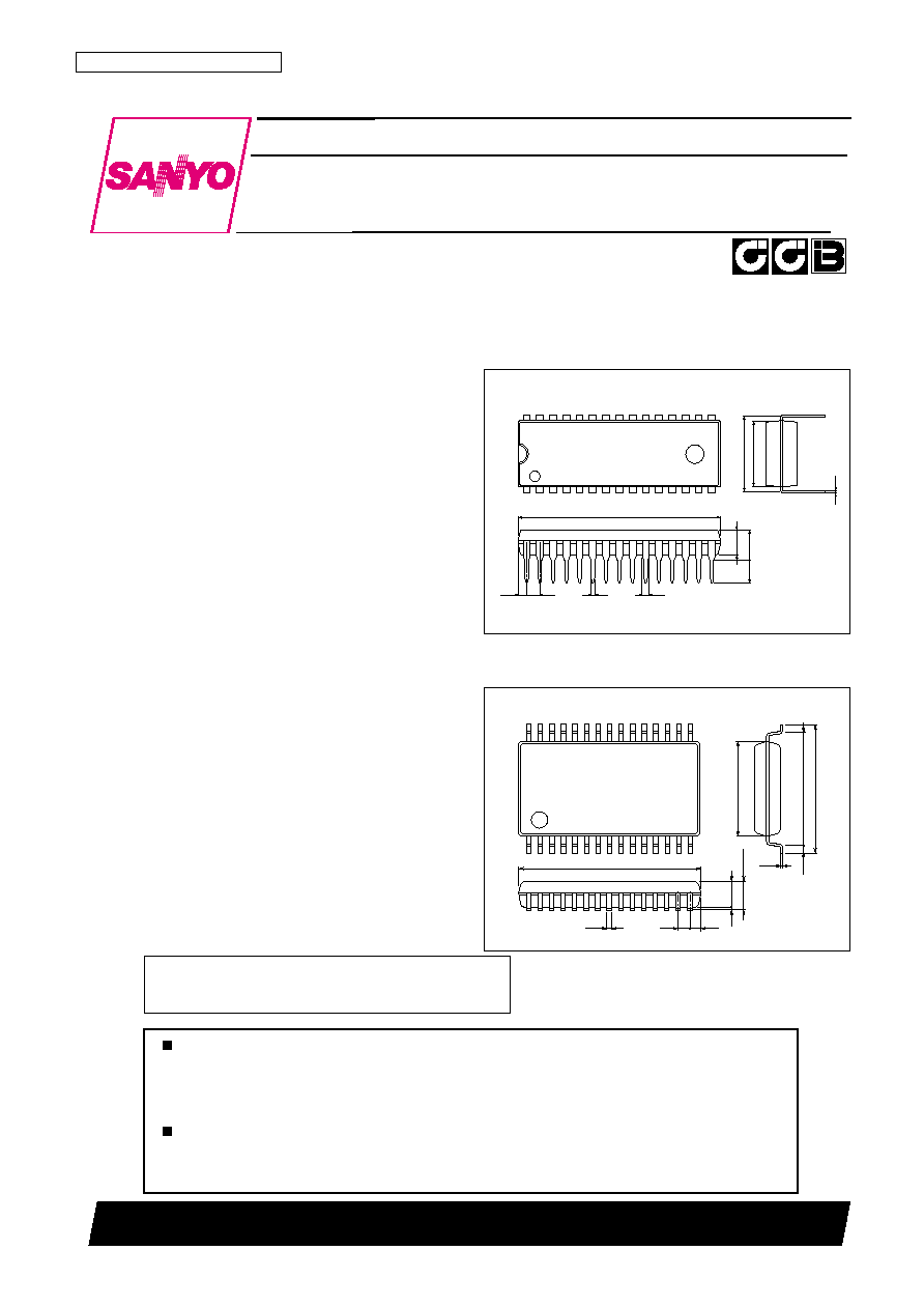
Package Dimensions
unit: mm
3196-DIP30SD
unit: mm
3216-MFP30S
1
15
30
16
1.14
1.78
27.2
0.25
10.16
8.6
0.48
0.95
3.25
3.0
3.95max
Preliminary
SANYO: DIP30SD
[LC75342]
0.15
15.3
1
15
30
16
0.65
1.0
0.35
2.5max
2.15
0.1
0.65
7.9
9.2
10.5
SANYO: MFP30S
[LC75342M]
LC75342, 75342M
SANYO Electric Co.,Ltd. Semiconductor Company
TOKYO OFFICE Tokyo Bldg., 1-10, 1 Chome, Ueno, Taito-ku, TOKYO, 110-8534 JAPAN
Single-Chip Volume and Tone Control System
CMOS IC
Any and all SANYO products described or contained herein do not have specifications that can handle
applications that require extremely high levels of reliability, such as life-support systems, aircraft's
control systems, or other applications whose failure can be reasonably expected to result in serious
physical and/or material damage. Consult with your SANYO representative nearest you before using
any SANYO products described or contained herein in such applications.
SANYO assumes no responsibility for equipment failures that result from using products at values that
exceed, even momentarily, rated values (such as maximum ratings, operating condition ranges, or other
parameters) listed in products specifications of any and all SANYO products described or contained
herein.
∑ CCB is a trademark of SANYO ELECTRIC CO., LTD.
∑ CCB is a SANYO's original bus format and all the
bus addresses are controlled by SANYO.
No. 6271-2/20
LC75342, 75342M
Specifications
Absolute Maximum Ratings
at Ta = 25∞C, V
SS
= 0 V
Parameter
Symbol
Pin
Conditions
Ratings
Unit
min
typ
max
Supply voltage
V
DD
V
DD
4.5
10
V
High-level input voltage
V
IH
CL, DI, CE
2.7
10
V
Low-level input voltage
V
IL
CL, DI, CE
7.5
V
DD
10.0
V
SS
1.0
V
4.5
V
DD
< 7.5
V
SS
0.8
Input voltage amplitude
V
IN
CE, DI, CL, L1 to L4,
V
SS
V
DD
Vp-p
R1 to R4, LIN, RIN
Input pulse width
t¯W
CL
1
µs
Setup time
tsetup
CL, DI, CE
1
µs
Hold time
thold
CL, DI, CE
1
µs
Operating frequency
fopg
CL
500
kHz
Allowable Operating Ranges
at Ta = ≠30 to +75∞C, V
SS
= 0 V
Parameter
Symbol
Pin
Conditions
Ratings
Unit
min
typ
max
Input resistance
Rin
L
IN
, R
IN
50
k
Volume Control Block
Parameter
Symbol
Pin
Conditions
Ratings
Unit
min
typ
max
Control range
Geq
max.boost
±18
±20
±22
dB
Step resolution
Estep
1
2
3
dB
Internal feedback resistance
Rfeed
66.6
k
Bass Band Equalizer Control Block
Parameter
Symbol
Pin
Conditions
Ratings
Unit
min
typ
max
Control range
Geq
max.boost/cut
±8
±10
±12
dB
Step resolution
Estep
1
2
3
dB
Internal feedback resistance
Rfeed
51.7
k
Treble Band Equalizer Control Block
Parameter
Symbol
Pin
Conditions
Ratings
Unit
min
typ
max
Maximum input gain
Gin max
+30
dB
Step resolution
Gstep
+2
dB
Input resistance
Rin
L1, L2, L3, L4
50
k
R1, R2, R3, R4
Clipping level
Vcl
LSEL0, RSEL0
THD = 1.0%, f = 1 kHz
2.90
Vrms
Output load resistance
Rl
LSEL0, RSEL0
10
k
Electrical Characteristics
at Ta = 25∞C, V
DD
= 9 V, V
SS
= 0 V
Input Block
Parameter
Symbol
Pin
Conditions
Ratings
Unit
Maximum supply voltage
V
DD
max
V
DD
11
V
Maximum input voltage
V
IN
max
CE, DI, CL, L1 to L4,
V
SS
≠ 0.3 to V
DD
+ 0.3
V
R1 to R4, LIN, RIN
Ta
75∞C
LC75342
450
Allowable power dissipation
Pdmax
Ta
75∞C
LC75342M
450
mW
with a PCB
*
Operating temperature
Topr
≠30 to +75
∞C
Storage temperature
Tstg
≠40 to +125
∞C
Note:
*
Printed circuit board size: 76.1
◊
114.3
◊
1.6 mm, printed circuit board material: glass/epoxy resin
No. 6271-3/20
LC75342, 75342M
Parameter
Symbol
Conditions
Ratings
Unit
min
typ
max
Total harmonic distortion
THD
V
IN
= 1 Vrms, f = 1 kHz, all flat overall
0.01
%
Crosstalk
CT
V
IN
= 1 Vrms, f = 1 kHz, Rg = 1 k
, all flat overall
80
dB
Output noise voltage
V
N
All flat overall, 80 kHz, L.P.F
9.3
µV
Maximum attenuation
Vomin
All flat overall, f = 1 kHz
≠90
dB
Current drain
I
DD
V
DD
≠ V
SS
= +10 V
37
mA
High-level input current
I
IH
CL, DI, CE: V
IN
= 10 V
10
µA
Low-level input current
I
IL
CL, DI, CE: V
IN
= 0 V
≠10
µA
Overall Characteristics
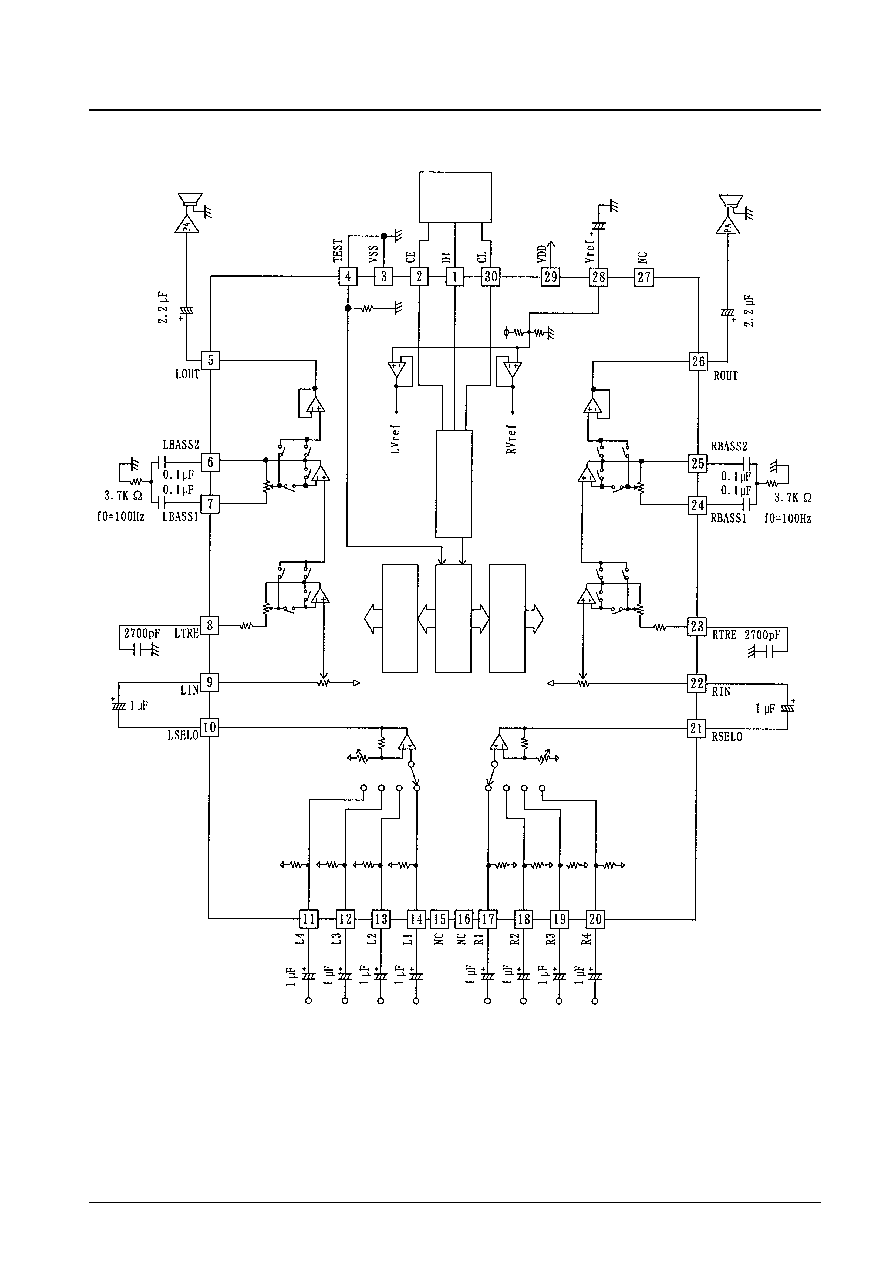
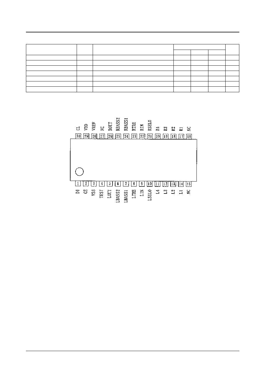
Pin Assignment
(Top view)
LC75342, 75342M
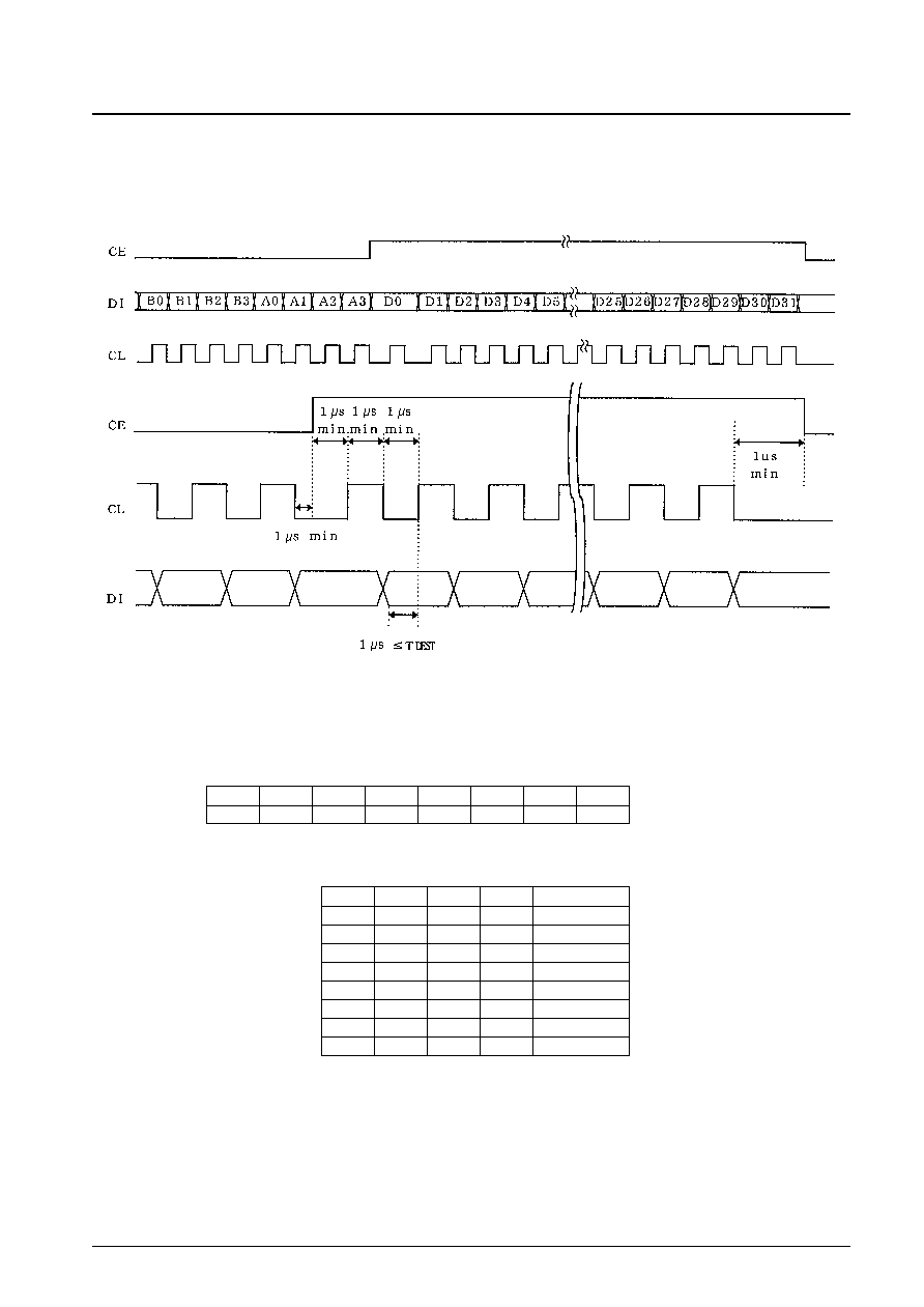
Control System Timing and Data Format
Applications control the LC75342 and LC75342M by applying the stipulated serial data to the CL, DI, and CE pins. This
data consists of a total of 40 bits, of which 8 bits are the address and 32 bits are the data itself.
∑ Address code (B0 to A3)
The LC75342 and LC75342M have an 8-bit address code, and can be used together with other ICs that support the
Sanyo CCB serial bus format.
Address code
(LSB)
(82HEX)
No. 6271-5/20
LC75342, 75342M
B0
B1
B2
B3
A0
A1
A2
A3
0
1
0
0
0
0
0
1
∑ Control code allocation
Input switching control
(L1, L2, L3, L4, R1, R2, R3, R4)
D0
D1
D2
D3
Operation
0
0
0
0
L1 (R1) ON
1
0
0
0
L2 (R2) ON
0
1
0
0
L3 (R3) ON
1
1
0
0
L4 (R4) ON
0
0
1
0
All switches off
1
0
1
0
All switches off
0
1
1
0
All switches off
1
1
1
0
All switches off