 | –≠–ª–µ–∫—Ç—Ä–æ–Ω–Ω—ã–π –∫–æ–º–ø–æ–Ω–µ–Ω—Ç: LC75347E | –°–∫–∞—á–∞—Ç—å:  PDF PDF  ZIP ZIP |
Ordering number : ENN
*
7378
D1503TN (OT) No. 7378 -1/17
Overview
The LC75347E is a 6-channel 97-step electronic volume
control system IC that provides a 2-channel input selector,
bass and treble tone controls, external output ports, and a
zero-cross volume switching function.
Functions
∑ Volume: 0 to ≠95 dB (in 1 dB steps) and ≠
, for a total
of 97 positions.
Each of the six input channels can be controlled
independently.
∑ Bass and treble: Each band can be controlled over a
±12 dB range in 2 dB steps.
The bass control provides peaking characteristics and
the treble control provides shelving characteristics.
∑ Selector: 2-channel input selector
∑ Zero cross: Provides independent zero-cross detection
for each of the 6 channels and a timer overflow
detection circuit.
∑ External muting: Mute in/mute out function using zero-
cross detection and dedicated pins.
∑ External output ports: Provides 4 n-channel transistor
open-drain outputs.
Features
∑ Built-in buffer amplifiers reduce the number of external
components to a minimum.
∑ Fabricated in a silicon-gate CMOS process for minimal
noise generation from internal switches.
∑ Built-in analog ground reference voltage generator
circuit
∑ All settings are controlled by serial data transmitted over
a CCB interface.
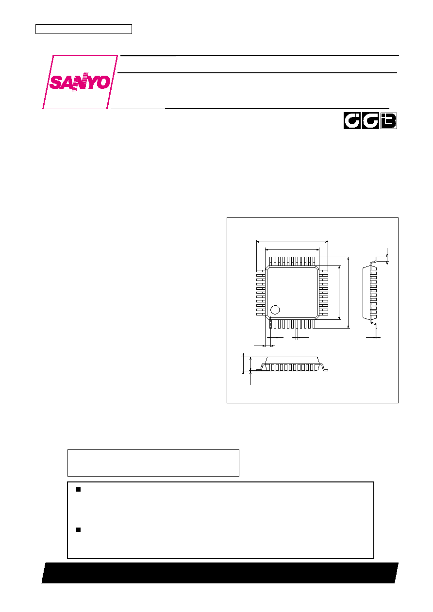
Package Dimensions
unit: mm
3148A-QIP44M
10.0
13.2
10.0
13.2
0.2
1.0
(2.5)
2.8max
0.1
0.35
0.8
(1.0)
1
44
Preliminary
SANYO: QIP44M
[LC75347E]
LC75347E
SANYO Electric Co.,Ltd. Semiconductor Company
TOKYO OFFICE Tokyo Bldg., 1-10, 1 Chome, Ueno, Taito-ku, TOKYO, 110-8534 JAPAN
Six-Channel Single-Chip Electronic Volume
Control System
CMOS LSI
Any and all SANYO products described or contained herein do not have specifications that can handle
applications that require extremely high levels of reliability, such as life-support systems, aircraft's
control systems, or other applications whose failure can be reasonably expected to result in serious
physical and/or material damage. Consult with your SANYO representative nearest you before using
any SANYO products described or contained herein in such applications.
SANYO assumes no responsibility for equipment failures that result from using products at values that
exceed, even momentarily, rated values (such as maximum ratings, operating condition ranges, or other
parameters) listed in products specifications of any and all SANYO products described or contained
herein.
∑ CCB is a trademark of SANYO ELECTRIC CO., LTD.
∑ CCB is SANYO's original bus format and all the bus
addresses are controlled by SANYO.
No. 7378 -2/17
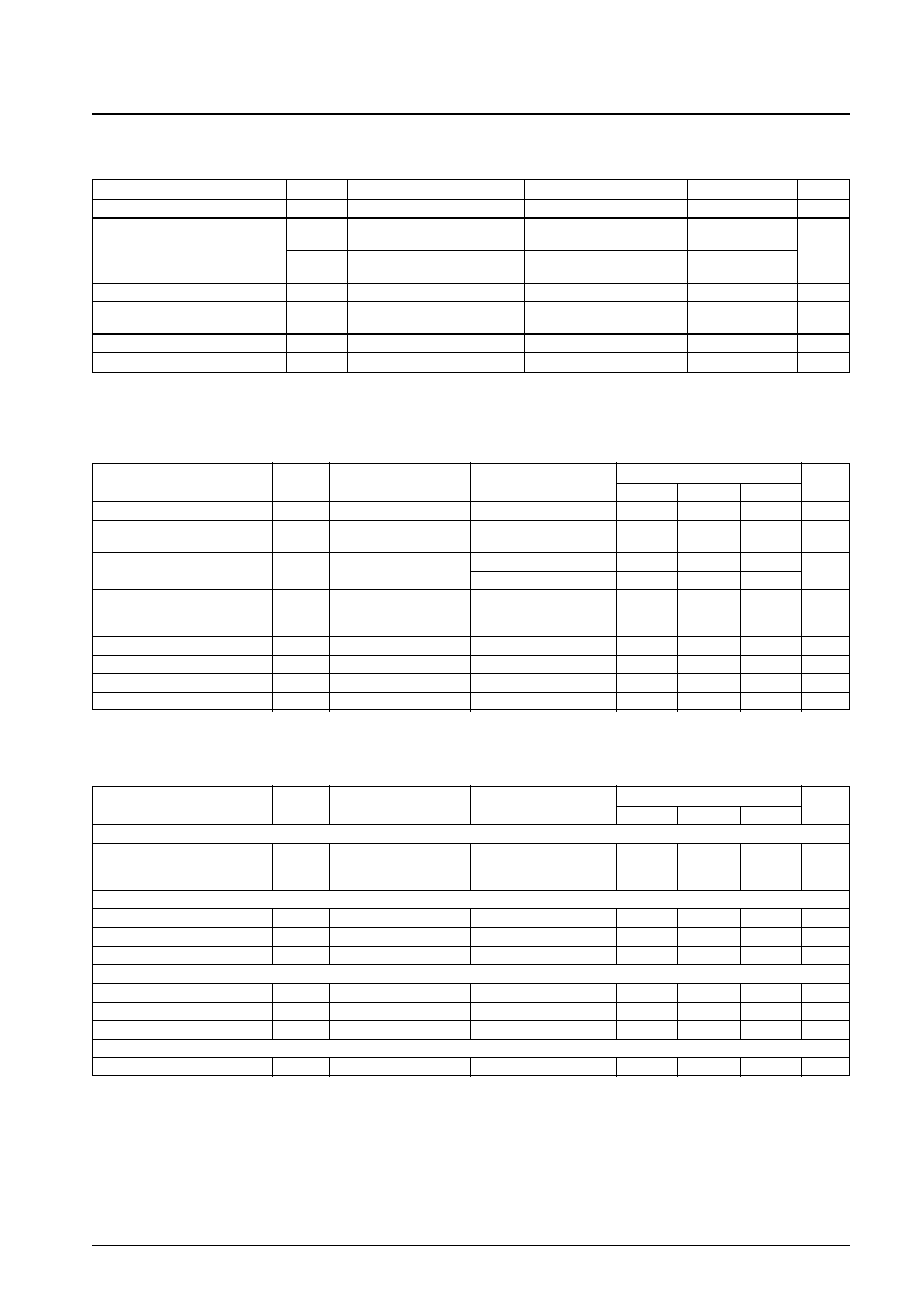
LC75347E
Parameter
Symbol
Pin
Conditions
Ratings
Unit
Maximum supply voltage
V
DD
max
V
DD
11
V
V
IN
1 max
CE, DI, CL, MUTE
≠0.3 to +11
Maximum input voltage
OUTP1 to OUTP4
V
V
IN
2 max
FL, FR, RL, RR, C, SBW, FLTON,
V
SS
≠ 0.3 to V
DD
+ 0.3
FRTON, FLIN, FRIN
Output current
I
OUT
OUTP1 to OUTP4
0 to 1
mA
Allowable power dissipation
Pdmax
Ta
85∞C
600
mW
*
1. When mounted on a PCB
Operating temperature
Topr
≠40 to +85
∞C
Storage temperature
Tstg
≠50 to +125
∞C
Specifications
Absolute Maximum Ratings
at Ta = 25∞C, V
SS
= 0 V
*
1: PCB dimensions: 76.1
◊
114.3
◊
1.6 mm, PCB materials: glass epoxy
Parameter
Symbol
Pin
Conditions
Ratings
Unit
min
typ
max
Supply voltage
V
DD
V
DD
4.5
10.5
V
High-level input voltage
V
IH
CL, DI, CE, MUTE
2.5
10.5
V
OUTP1 to OUTP4
Low-level input voltage
V
IL
CL, DI, CE, MUTE
7.5
V
DD
10.5
V
SS
0.8
V
4.5
V
DD
< 7.5
V
SS
0.3
FL, FR, RL, RR, C, SBW,
Input amplitude
V
IN
FLTON, FRTON, FLIN,
V
SS
V
DD
Vp-p
FRIN
Input pulse width
t¯W
CL
1
µs
Setup time
tsetup
CL, DI, CE
1
µs
Hold time
thold
CL, DI, CE
1
µs
Operating frequency
fopg
CL
500
kHz
Allowable Operating Ranges
at Ta = ≠40 to +85∞C, V
SS
= 0 V
Parameter
Symbol
Pin
Conditions
Ratings
Unit
min
typ
max
[Volume and Selector Blocks]
FL, FR, RL, RR, C, SBW,
Input resistance
Rin
FLTON, FRTON, FLIN,
50
k
FRIN
[Treble Band Equalizer Control Block]
Control range
Geq
max. boost/cut
±10
±12
±14
dB
Step resolution
Estep
1
2
3
dB
Internal feedback resistance
Rfeed
51.7
k
[Bass Band Equalizer Control Block]
Control range
Geq
max. boost/cut
±10
±12
±14
dB
Step resolution
Estep
1
2
3
dB
Internal feedback resistance
Rfeed
38.9
k
[Output Port Block]
Low-level output voltage
V0
OUTP1 to OUTP4
Rh = 10 k
, Vd = 5 V
0.5
V
Electrical Characteristics
at Ta = 25∞C, V
DD
= 9 V, V
SS
= 0 V
Continued on next page.
No. 7378 -3/17
LC75347E
Continued from preceding page.
Parameter
Symbol
Conditions
Ratings
Unit
min
typ
max
[Overall Characteristics]
Total harmonic distortion (RL, RR, C and
THD1
V
IN
= 1 Vrms, f = 1 kHz, 80 kHz LPF
0.001
0.01
SBW inputs, direct output)
Flat overall
Total harmonic distortion (FL and FR inputs,
V
IN
= 1 Vrms, f = 1 kHz, 80 kHz LPF
direct output)
THD2
Flat overall
0.002
0.01
FL and FR selected, direct output
%
Total harmonic distortion (FLTON and FRTON
V
IN
= 1 Vrms, f = 1 kHz, 80 kHz LPF
inputs, FLOUT and FROUT outputs)
THD3
Flat overall
0.003
0.01
FLTON and FRTON selected, output after
passing though tone controls.
80 kHz LPF, Rg = 1 k
6
Output noise voltage (RL, RR, C and SBW
VN1
All controls flat overall
inputs, direct output)
A-WIGHT, Rg = 1 k
2.5
All controls flat overall
80 kHz LPF, Rg = 1 k
7
Output noise voltage (FL and FR inputs,
VN2
All controls flat overall
µV
direct output)
A-WIGHT, Rg = 1 k
3
All controls flat overall
80 kHz LPF, Rg = 1 k
9
Output noise voltage (FLTON and FRTON
VN3
All controls flat overall
inputs, FLOUT and FROUT outputs)
A-WIGHT, Rg = 1 k
4
All controls flat overall
Characteristics at maximum attenuation
Vomin
V
IN
= 1 Vrms, f = 1 kHz, 80 kHz LPF
≠95
dB
All controls flat overall
Crosstalk
CT
V
IN
= 1 Vrms, f = 1 kHz, Rg = 1 k
80
dB
All controls flat overall
Current drain
I
DD
V
DD
≠ V
SS
= +9 V
38
mA
High-level input current
I
IH
CL, DI, CE, MUTE: V
IN
= 10.5 V,V
DD
= 10.5 V
10
µA
Low-level input current
I
IL
CL, DI, CE, MUTE: V
IN
= 0 V,V
DD
= 10.5 V
≠10
µA
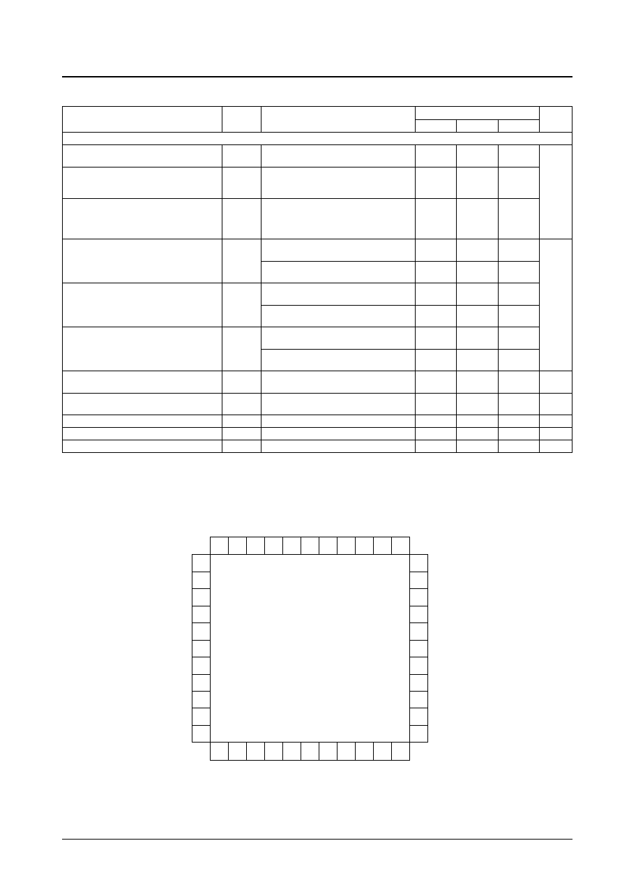
Pin Assignment
MUTE
43
44
SELL
FLIN
OUTP4
37
39
40
5
7
VREF
FRTON
SELR
TRE2
BASS21
BASS22
FRIN
NC
FR
29
OUTP3
36
OUTP2
35
34
VSS
OUTP1
FLTON
33
32
23
28
31
30
BASS23
FL
C
21 NC
22
27
26
25
24
20
RR
CL
38
TIM
RL
17 NC
19 NC
18
NC
13 RROUT
VDD
42
14 SBWOUT
CE
41
DI
8
1
2
3
4
6
9
10
11
NC: No Connect
Top view
16 SBW
12 RLOUT
15
COUT
TRE1
BASS11
BASS12
BASS13
NC
FLOUT
FROUT
LC75347E
QIP44M

Equivalent Circuit/Application Circuit Example
No. 7378 -4/17
LC75347E
NC
NC
NC
NC
VREF
27
3
2
5
TRE2
BASS23
29
BASS21
31
FLOUT
20
1
RROUT
RR
7
6
14
10
BASS22
OUTP4
SBW
44
38
FLIN
OUTP3
VSS
OUTP1
TRE1
43
42
4
OUTP2
COUT
12
26
16
21
17
15
13
18
11
8
C
RL
19
22
23
25
24
BASS11
BASS13
BASS12
SELL
MUTE
37
40
39
CL
DI
CE
TIM
VDD
34
33
RLOUT
NC
SBWOUT
35
36
FROUT
9
41
FLTON
FR
SELR
FRIN
FRTON
FL
28
NC
32
30
NO SIGNAL
TIMER
CONTROL
CIRCUIT
LOGIC
CIRCUIT
CCB
INTERFACE
µ
COM
6.5 k
0.1
µ
F
0
.1
µ
F
6.5 k
50 k
50 k
2700 pF
1
µ
F
5 V
0.033
µ
F
2.2
µ
F
ZERO-CROSS
DETECTOR
2700 pF
10 k
10 k
10 k
1
µ
F
1
µ
F
1
µ
F
1
µ
F
2.2
µ
F
20 k
20 k
22
µ
F
1
µ
F
1 M
47 k
2.2
µ
F
2.2
µ
F
2.2
µ
F
2.2
µ
F
0.1
µ
F
0.1
µ
F
1
µ
F
1
µ
F
1
µ
F
1
µ
F
50 k
50 k
10 k
5V
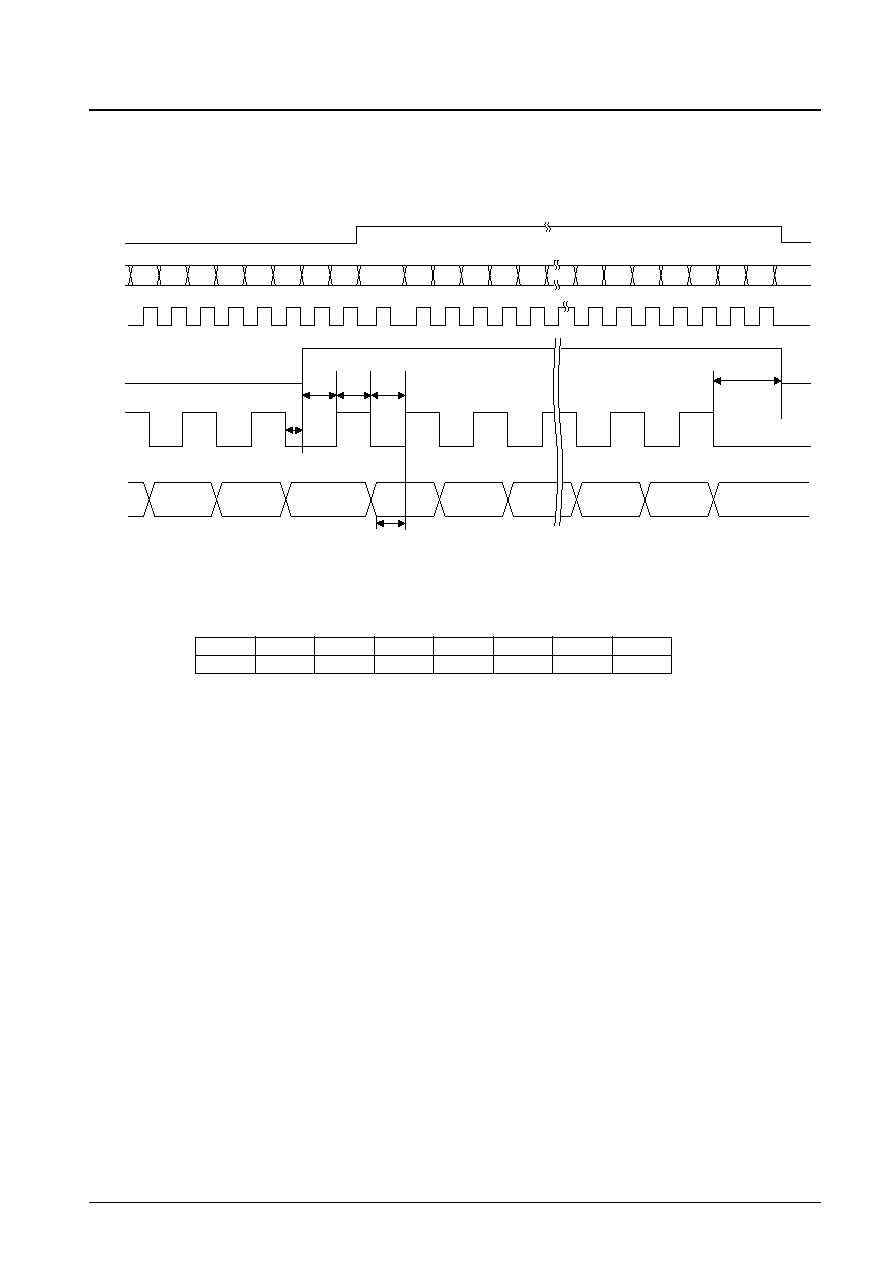
Control System Timing and Data Format
The stipulated serial data must be applied to the CL, DI, and CE pins to control the LC75347E. The data consists of 80
bits, of which 8 bits are address and 72 bits are data.
∑ Address Code (B0 to A3)
This IC has an 8-bit address code and can be used with the same specifications as other Sanyo CCB serial bus ICs.
Address code
(LSB) (82HEX)
No. 7378 -5/17
LC75347E
D65 D66 D67 D68 D69 D70 D71
D0
D5
D4
D3
D2
D1
A3
A2
A1
A0
B3
B2
B1
B0
CL
DI
CE
1
µ
s
min
1
µ
s
min
1
µ
s
min
1
µ
s
min
1
µ
s
min
1
µ
s
T
DEST
DI
CL
CE
B0
B1
B2
B3
A0
A1
A2
A3
0
1
0
0
0
0
0
1
∑ Control Code Allocations
Volume Control
No. 7378 -6/17
LC75347E
D0
D1
D2
D3
D4
D5
D6
D7
SBW setting
D8
D9
D10
D11
D12
D13
D14
D15
RR setting
D16
D17
D18
D19
D20
D21
D22
D23
RL setting
D24
D25
D26
D27
D28
D29
D30
D31
C setting
D32
D33
D34
D35
D36
D37
D38
D39
FRIN setting
D40
D41
D42
D43
D44
D45
D46
D47
FLIN setting
0
0
0
0
0
0
0
0
0 dB
1
0
0
0
0
0
0
0
≠1 dB
0
1
0
0
0
0
0
0
≠2 dB
1
1
0
0
0
0
0
0
≠3 dB
0
0
1
0
0
0
0
0
≠4 dB
1
0
1
0
0
0
0
0
≠5 dB
0
1
1
0
0
0
0
0
≠6 dB
1
1
1
0
0
0
0
0
≠7 dB
0
0
0
1
0
0
0
0
≠8 dB
1
0
0
1
0
0
0
0
≠9 dB
0
1
0
1
0
0
0
0
≠10 dB
1
1
0
1
0
0
0
0
≠11 dB
0
0
1
1
0
0
0
0
≠12 dB
1
0
1
1
0
0
0
0
≠13 dB
0
1
1
1
0
0
0
0
≠14 dB
1
1
1
1
0
0
0
0
≠15 dB
0
0
0
0
1
0
0
0
≠16 dB
1
0
0
0
1
0
0
0
≠17 dB
0
1
0
0
1
0
0
0
≠18 dB
1
1
0
0
1
0
0
0
≠19 dB
0
0
1
0
1
0
0
0
≠20 dB
1
0
1
0
1
0
0
0
≠21 dB
0
1
1
0
1
0
0
0
≠22 dB
1
1
1
0
1
0
0
0
≠23 dB
0
0
0
1
1
0
0
0
≠24 dB
1
0
0
1
1
0
0
0
≠25 dB
0
1
0
1
1
0
0
0
≠26 dB
1
1
0
1
1
0
0
0
≠27 dB
0
0
1
1
1
0
0
0
≠28 dB
1
0
1
1
1
0
0
0
≠29 dB
0
1
1
1
1
0
0
0
≠30 dB
1
1
1
1
1
0
0
0
≠31 dB
0
0
0
0
0
1
0
0
≠32 dB
1
0
0
0
0
1
0
0
≠33 dB
0
1
0
0
0
1
0
0
≠34 dB
1
1
0
0
0
1
0
0
≠35 dB
0
0
1
0
0
1
0
0
≠36 dB
1
0
1
0
0
1
0
0
≠37 dB
0
1
1
0
0
1
0
0
≠38 dB
1
1
1
0
0
1
0
0
≠39 dB
0
0
0
1
0
1
0
0
≠40 dB
1
0
0
1
0
1
0
0
≠41 dB
0
1
0
1
0
1
0
0
≠42 dB
1
1
0
1
0
1
0
0
≠43 dB
0
0
1
1
0
1
0
0
≠44 dB
1
0
1
1
0
1
0
0
≠45 dB
0
1
1
1
0
1
0
0
≠46 dB
Continued on next page.
No. 7378 -7/17
LC75347E
Continued from preceding page.
D0
D1
D2
D3
D4
D5
D6
D7
SBW setting
D8
D9
D10
D11
D12
D13
D14
D15
RR setting
D16
D17
D18
D19
D20
D21
D22
D23
RL setting
D24
D25
D26
D27
D28
D29
D30
D31
C setting
D32
D33
D34
D35
D36
D37
D38
D39
FRIN setting
D40
D41
D42
D43
D44
D45
D46
D47
FLIN setting
1
1
1
1
0
1
0
0
≠47 dB
0
0
0
0
1
1
0
0
≠48 dB
1
0
0
0
1
1
0
0
≠49 dB
0
1
0
0
1
1
0
0
≠50 dB
1
1
0
0
1
1
0
0
≠51 dB
0
0
1
0
1
1
0
0
≠52 dB
1
0
1
0
1
1
0
0
≠53 dB
0
1
1
0
1
1
0
0
≠54 dB
1
1
1
0
1
1
0
0
≠55 dB
0
0
0
1
1
1
0
0
≠56 dB
1
0
0
1
1
1
0
0
≠57 dB
0
1
0
1
1
1
0
0
≠58 dB
1
1
0
1
1
1
0
0
≠59 dB
0
0
1
1
1
1
0
0
≠60 dB
1
0
1
1
1
1
0
0
≠61 dB
0
1
1
1
1
1
0
0
≠62 dB
1
1
1
1
1
1
0
0
≠63 dB
0
0
0
0
0
0
1
0
≠64 dB
1
0
0
0
0
0
1
0
≠65 dB
0
1
0
0
0
0
1
0
≠66 dB
1
1
0
0
0
0
1
0
≠67 dB
0
0
1
0
0
0
1
0
≠68 dB
1
0
1
0
0
0
1
0
≠69 dB
0
1
1
0
0
0
1
0
≠70 dB
1
1
1
0
0
0
1
0
≠71 dB
0
0
0
1
0
0
1
0
≠72 dB
1
0
0
1
0
0
1
0
≠73 dB
0
1
0
1
0
0
1
0
≠74 dB
1
1
0
1
0
0
1
0
≠75 dB
0
0
1
1
0
0
1
0
≠76 dB
1
0
1
1
0
0
1
0
≠77 dB
0
1
1
1
0
0
1
0
≠78 dB
1
1
1
1
0
0
1
0
≠79 dB
0
0
0
0
1
0
1
0
≠80 dB
1
0
0
0
1
0
1
0
≠81 dB
0
1
0
0
1
0
1
0
≠82 dB
1
1
0
0
1
0
1
0
≠83 dB
0
0
1
0
1
0
1
0
≠84 dB
1
0
1
0
1
0
1
0
≠85 dB
0
1
1
0
1
0
1
0
≠86 dB
1
1
1
0
1
0
1
0
≠87 dB
0
0
0
1
1
0
1
0
≠88 dB
1
0
0
1
1
0
1
0
≠89 dB
0
1
0
1
1
0
1
0
≠90 dB
1
1
0
1
1
0
1
0
≠91 dB
0
0
1
1
1
0
1
0
≠92 dB
1
0
1
1
1
0
1
0
≠93 dB
0
1
1
1
1
0
1
0
≠94 dB
1
1
1
1
1
0
1
0
≠95 dB
1
1
1
1
1
1
1
0
≠

No. 7378 -8/17
LC75347E
Zero cross control
D48
SBW setting
D49
RR setting
D50
RL setting
Operation
D51
C setting
D52
FRIN setting
D53
FLIN setting
0
Zero cross operation
1
Zero cross operation is disabled (This setting takes effect on the fall of CE.)
Tone Switch Selection
D54
D55
Setting
0
0
The analog switches are set so that FL and FR bypass the tone circuit.
1
0
The analog switches are set so that FL is connected to, and FR bypass the tone circuit.
0
1
The analog switches are set so that FR is connected to, and FL bypass the tone circuit.
1
1
The analog switches are set so that FL and FR are connected to the tone circuit.
Tone Mode
D64
D65
Setting
0
0
FLTON and FRTON not changed
1
0
Only FLTON changed
0
1
Only FRTON changed
1
1
Both FLTON and FRTON changed
Test Mode
D70
D71
Setting
0
0
These bits are used for IC testing. They must be set to 0 during normal operation.
Output Ports
Setting
D66
OUTP1 (VSS: 1, OPEN: 0)
D67
OUTP2 (VSS: 1, OPEN: 0)
D68
OUTP3 (VSS: 1, OPEN: 0)
D69
OUTP4 (VSS: 1, OPEN: 0)
Bass
D56
D57
D58
D59
FLTON setting
FRTON setting
0
1
1
0
+12 dB
1
0
1
0
+10 dB
0
0
1
0
+8 dB
1
1
0
0
+6 dB
0
1
0
0
+4 dB
1
0
0
0
+2 dB
0
0
0
0
0 dB
1
0
0
1
≠2 dB
0
1
0
1
≠4 dB
1
1
0
1
≠6 dB
0
0
1
1
≠8 dB
1
0
1
1
≠10 dB
0
1
1
1
≠12 dB
Treble
D60
D61
D62
D63
FLTON setting
FRTON setting
0
1
1
0
+12 dB
1
0
1
0
+10 dB
0
0
1
0
+8 dB
1
1
0
0
+6 dB
0
1
0
0
+4 dB
1
0
0
0
+2 dB
0
0
0
0
0 dB
1
0
0
1
≠2 dB
0
1
0
1
≠4 dB
1
1
0
1
≠6 dB
0
0
1
1
≠8 dB
1
0
1
1
≠10 dB
0
1
1
1
≠12 dB
No. 7378 -9/17
LC75347E
Pin Functions
Pin No.
Pin
Function
Notes
∑ Volume control inputs
7
24
20
18
22
16
FLIN
FRIN
RL
RR
C
SBW
VDD
∑ Volume control outputs
9
10
11
12
13
14
FLOUT
FROUT
COUT
RLOUT
RROUT
SBWOUT
VDD
FLOUT
FROUT
RLOUT
RROUT
COUT
SBWOUT
∑ Selector volume inputs
28
26
FL
FR
VDD
FL
RL
VREF
SELL
SELR
From TONE
∑ Selector volume outputs
6
25
SELL
SELR
VDD
VDD
∑ Zero cross circuit timer
If a zero cross is not detected during the period from the
completion of the data transfer to the point the timer
overflows, the control data is enabled forcibly.
36
TIM
VDD
VREF
VDD
∑ 0.5
◊
V
DD
voltage generator used for analog ground
A capacitor of several ten µF must be connected between
VREF and V
SS
to minimize power supply ripple.
23
VREF
∑ Ground
41
V
SS
∑ Power supply
37
V
DD
∑ Chip enable
Data is written to the internal latch when this pin goes from
high to low. The analog switches operate at that time. Data
transfer is enabled when CE is high.
40
CE
∑ Serial data and clock inputs for the control data.
39
38
DI
CL
Continued on next page.
No. 7378 -10/17
LC75347E
Continued from preceding page.
Pin No.
Pin
Function
Notes
∑ External control mute pin
Applying the V
SS
level to this pin forcibly sets the volume
level for all channels to ≠
.
35
MUTE
VDD
∑ Tone control block inputs
After passing through the tone control circuit, the audio
signals are output to the selector amplifier.
34
33
FLTON
FRTON
BASS11
BASS21
VDD
VREF
FLTON
FRTON
VDD
VDD
BASS13
BASS23
VDD
VREF
∑ Connections for the capacitors that form the bass filters
3
5
31
29
BASS11
BASS13
BASS21
BASS23
∑ Connections for the resistors that form the bass filters
4
30
BASS12
BASS22
TRE1
TRE2
VDD
VDD
∑ Connections for the capacitors that form the treble filters
2
32
TRE1
TRE2
OUTP1
OUTP2
OUTP3
OUTP4
∑ N-channel transistor open-drain outputs
When off, these outputs are in the high-impedance state.
1
44
43
42
OUTP1
OUTP2
OUTP3
OUTP4
∑ Unused pins
These pins must either be left open or connected to V
SS
.
8
15
17
19
21
27
NC
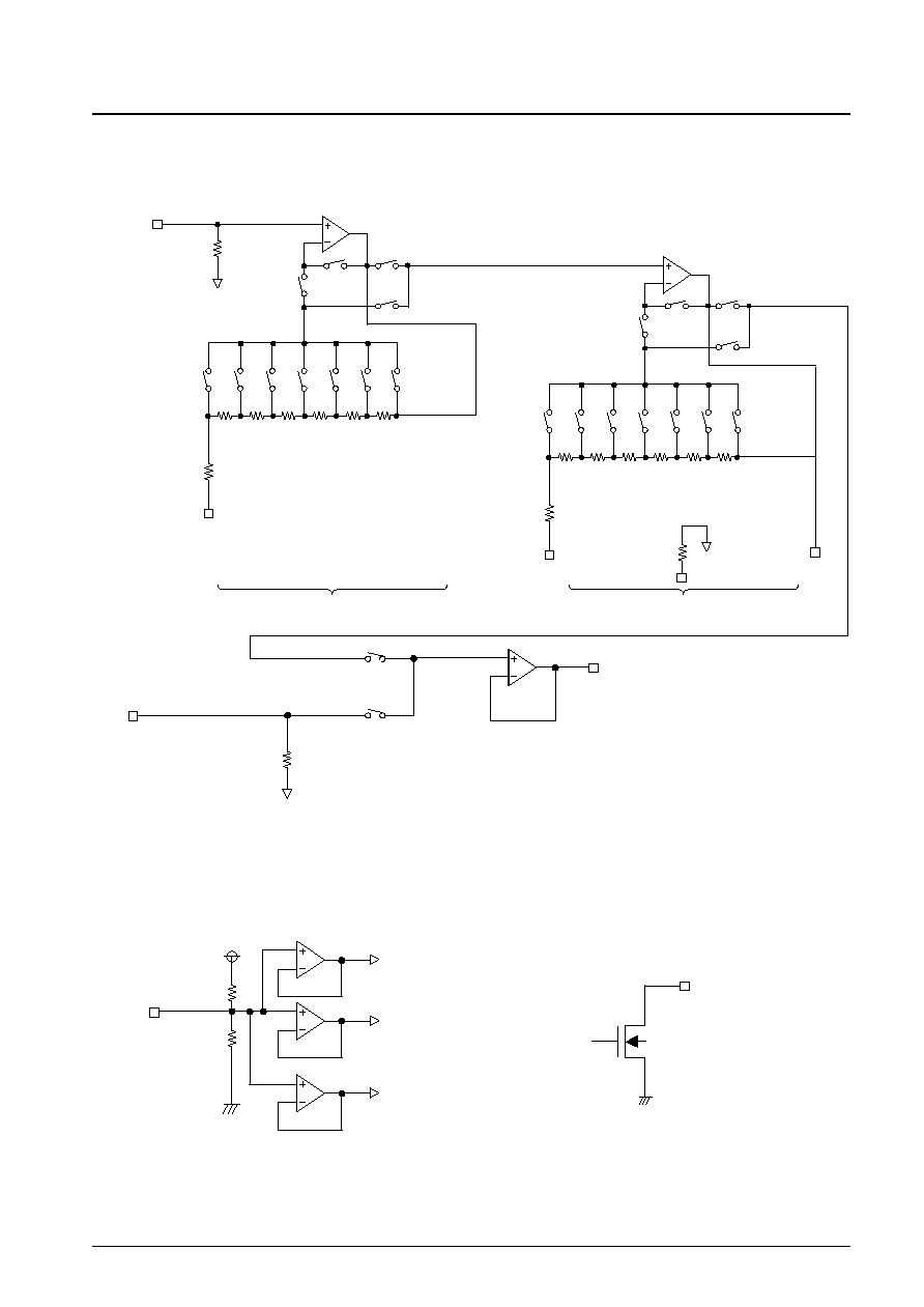
Internal Equivalent Circuits
∑ Selector, Bass/Treble, VREF Amplifier, Output Ports
No. 7378 -11/17
LC75347E
FRTON is identical.
Units (Resistance: k
)
For boost, set switches 1 and 3 to the on position, for cut, set switches 2 and 4 to the on position,
and for 0 dB, set switches 2, 3 and 0 dB switch to the on position.
FLTON
TRE1
Total= 51.674
SW3
SW4
SW2
SW1
0
.
0
2
7
3
.
3
7
3
4
.
2
4
6
5
.
3
4
6
6
.
7
3
0
8
.
4
7
3
1
0
.
6
6
6
SW3
SW4
SW2
SW1
FL
SELL
50
VREF
VDD
20
20
VREF1
VREF2
VREF3
BASS11
Total= 38.861
±
1
2
d
B
±
1
0
d
B
±
8
d
B
±
6
d
B
±
4
d
B
±
2
d
B
±
0
d
B
1
2
.
8
4
0
3
.
3
7
3
4
.
2
4
6
5
.
3
4
6
6
.
7
3
0
8
.
4
7
3
1
0
.
6
6
6
BASS13
±
1
2
d
B
±
1
0
d
B
±
8
d
B
±
6
d
B
±
4
d
B
±
2
d
B
±
0
d
B
OUTP1
OUTP2 to 4 are identical.
50
6.5
BASS12
VREF
VREF
VREF
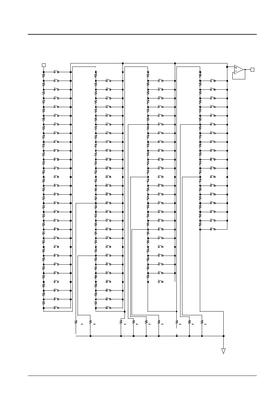
∑ Volume Block
Total resistance: 50 k
(Parallel resistors)
No. 7378 -12/17
LC75347E
VREF
R104
808
R105
810
R103
806
R101
802
FLIN
FLOUT
R98
Resistor units:
FRIN, RL, RR, C and SBW are identical.
796
R97
794
R100
800
R99
798
R102
804
R95=
55
≠95dB
R96=
450
≠
dB
R93=
69
≠93dB
R94=
62
≠94dB
R91=
87
≠91dB
R92=
78
≠92dB
R89=
55
≠89dB
R90=
49
≠90dB
R87=
69
≠87dB
R88=
62
≠88dB
R85=
87
≠85dB
R86=
78
≠86dB
R83=
55
≠83dB
R84=
49
≠84dB
R81=
69
≠81dB
R82=
62
≠82dB
R79=
87
≠79dB
R80=
78
≠80dB
R78=
49
≠78dB
R76=
62
≠76dB
R77=
55
≠77dB
R74=
78
≠74dB
R75=
69
≠75dB
R72=
49
≠72dB
R73=
87
≠73dB
R70=
62
≠70dB
R71=
55
≠71dB
R68=
78
≠68dB
R69=
69
≠69dB
R66=
49
≠66dB
R67=
86
≠67dB
R64=
62
≠64dB
R65=
55
≠65dB
R62=
78
≠62dB
R63=
69
≠63dB
R60=
49
≠60dB
R61=
86
≠61dB
R58=
61
≠58dB
R59=
55
≠59dB
≠52dB
≠53dB
≠54dB
≠30dB
≠31dB
≠32dB
≠33dB
≠34dB
≠35dB
≠36dB
≠48dB
≠49dB
≠50dB
≠51dB
≠44dB
≠45dB
≠46dB
≠47dB
≠40dB
≠41dB
≠42dB
≠43dB
≠37dB
≠38dB
≠39dB
R29=
R30=
R39=
68
R35=
108
R36=
≠28dB
≠29dB
R55=
86
R56=
77
≠55dB
≠56dB
R57=
69
≠57dB
R53=
55
R54=
49
R51=
69
R52=
61
R49=
86
R50=
77
R47=
55
R48=
49
R45=
69
R46=
61
R43=
86
R44=
77
R41=
55
R42=
48
R40=
61
R37=
86
R38=
77
97
R33=
137
R34=
122
≠24dB
≠25dB
≠26dB
≠27dB
≠20dB
≠21dB
≠22dB
≠23dB
≠16dB
≠17dB
≠18dB
≠19dB
≠13dB
≠12dB
≠14dB
≠15dB
R27=
273
0dB
≠1dB
≠2dB
≠3dB
≠4dB
≠5dB
≠6dB
≠7dB
R25=
343
R26=
306
R23=
432
R24=
385
R21=
544
R22=
485
R19=
685
R20=
610
R17=
862
R18=
768
R15= 1085
R16=
967
R13= 1366
R14= 1218
R11= 1720
R12= 1533
R9=
2165
R10= 1930
R7=
2726
R8=
2429
R2=
R3=
R6=
4845
4319
3850
3431
3058
R4=
R5=
R31=
R32=
≠8dB
≠9dB
R1=
5434
≠11dB
193
243
216
172
153
≠10dB
R28=
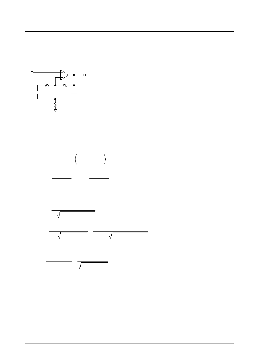
Calculating the Equalizer External Component Values
1. Bass Band Circuit
Here we show the equivalent circuit and the formulas for calculating the capacitor and resistor values for a center
frequency of 100 Hz.
∑ Bass band equivalent circuit
∑ Sample calculation
Specifications: Center frequency, f
0
= 100 Hz
Gain at maximum boost: G = 12 dB
Assume R1 = 27
, R2 = 38,834
, and C1 = C2 = C.
(1) Determine R3 from the fact that G = 12 dB.
(2) Determine C from the fact that the center frequency, f
0
, is 100 Hz.
(3) Determine Q.
No. 7378 -13/17
LC75347E
R1
R2
R3
C2
C1
2R3 + R1
R2
G
+12dB
= 20
◊
LOG
10
1 +
=
6500
2
≠ 27
(3.981 ≠ 1)
38834
2
(10
G/20
≠1)
≠R1
R2
R3 =
(R1 + R2) R3C1C2
2
1
f
0
=
C =
0.1
µ
F
(38834 + 27)
◊
6500
2
◊
100
1
(R1 + R2) R3
2
f
0
1
=
1.22
∑
(R1 + R2) R3
1
2R3 + R1
(R1 + R2) R3
Q =
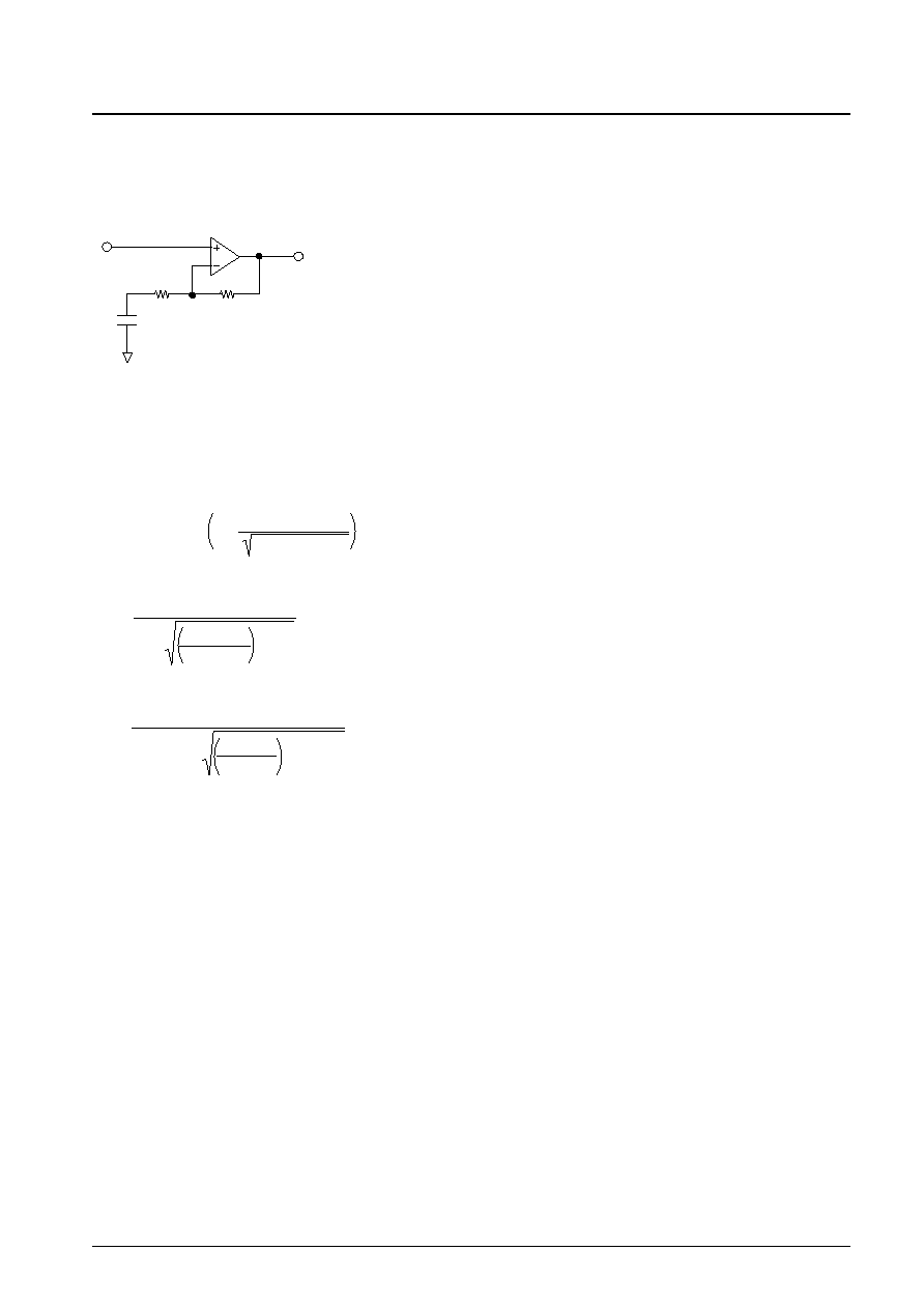
2. Treble Band Circuit
The treble band circuit can provide shelving characteristics. Here we present the equivalent circuit when the circuit is
providing boost and the circuit calculation formulas.
∑ Treble band equivalent circuit
∑ Sample calculation
Specifications: Set frequency, f = 26,000 Hz
Gain at maximum boost: G
+12 dB
= 12 dB
Assume R1 = 12,840
and R2 = 38,834
.
Substituting the above values into the following formulas allows us to solve for C.
No. 7378 -14/17
LC75347E
R1
R2
C
G = 20
◊
LOG
10
1 +
R2
R1
2
+ (1/
C)
2
C
R2
≠ R1
2
=
1
2
f
10
G/20
≠ 1
2
2700 (pF)
≠ 12840
2
3.98 ≠ 1
38834
2
26000
1
=
2

No. 7378 -15/17
LC75347E
Usage Notes
1. Data Transmission after Power is First Applied
The states of the internal analog switches are undefined when power is first applied. Applications should set up the
initial data immediately after power is applied (after V
DD
rises above 4.5 V). Applications should also mute the
outputs until the data has been set up and the outputs are stable.
To establish the states of the internal latches, set the bits D64 and D65 to 1 in the first data transferred after power is
first applied.
2. Zero Cross Switching Control
Zero cross switching is used by setting up data in which the zero cross control bits specify zero cross detection mode
(by setting bits D48 to D53 to 0) and transfer that data. Since these control bits are latched first, immediately after the
data is transferred, that is, on the fall of the CE signal, zero cross control can be performed with a single data transfer
operation when updating the volume control settings. If the zero cross control bits specify zero cross detection
disabled mode (by setting bits D48 to D53 to 1), the volume is switched on the fall of the CE signal at the end of the
data transfer.
3. Zero Cross Timer Setting
When the input signal is less than the detection sensitivity of the zero cross comparator, or if only a low-frequency
signal is being input, the state where the IC does not detect a zero cross will continue and the data will not be latched.
The zero cross timer allows applications to set a time at which data will be latched forcibly if the state where no zero
cross is detected continues.
For example, to set a time of 25 ms:
T = 0.69CR
Since the internal pull-up resistor is about 1 M
:
Applications usually set a time in the range 10 to 50 ms.
4. Notes on Serial Data Transfer
Cover the CL, DI, and CE pin signal lines with the ground pattern, or use shielded cables for these signals so that the
high-frequency digital signals transmitted on these lines do not enter the analog signal system.
C =
0.036
µ
F
25
◊
10
≠3
0.69
◊
1.0
◊
10
6
No. 7378 -16/17
LC75347E
Output
--
dB
Step -- dB
Bass Tone Control Characteristics
Output le
v
el
--
dBV
Frequency, f -- Hz
ILC05496
--40
--35
--30
--25
--20
--15
--10
--5
0
100k
2 3
5 7
10k
2 3
5 7
1k
2 3
5 7
100
10
2 3
5 7
VDD = 9 V
VIN = --20 dBV
Volume Control Step Characteristics
ILC05489
--100
--90
--80
--70
--60
--50
--40
--30
--20
--10
0
--70
--60
--50
--100
--90
--80
--40
--30
--20
--10
0
VDD = 9 V
VIN = 0 dBV
f = 1 kHz
Frequency, f -- Hz
Distortion vs. Frequency Characteristics (1)
Distortion
--
%
ILC05490
7
5
3
3
2
0.001
0.01
2
100k
2 3
5 7
10k
2 3
5 7
1k
2 3
5 7
100
10
2 3
5 7
VIN = --10 dBV
VIN = 0 dBV
Frequency, f -- Hz
Distortion vs. Frequency Characteristics (2)
Distortion
--
%
ILC05491
7
5
7
5
3
3
2
0.001
100k
2 3
5 7
10k
2 3
5 7
1k
2 3
5 7
100
10
2 3
5 7
VIN= --10 dBV
VIN = 0 dBV
Input level -- dBV
Distortion vs. Input Level Characteristics (1)
Distortion
--
%
ILC05492
7
5
3
2
2
0.1
7
5
7
3
2
0.01
0.001
--40
--30
--20
--10
0
10
1 kHz
10 kHz
Input level -- dBV
Distortion vs. Input Level Characteristics (2)
Distortion
--
%
ILC05493
7
5
3
2
0.1
7
5
3
7
5
3
2
0.01
0.001
--40
--30
--20
--10
0
--35
--25
--15
--5
5
10
10 kHz
1 kHz
Supply voltage -- V
Distortion vs. Supply Voltage (1)
Distortion
--
%
ILC05494
3
2
7
5
3
7
5
2
0.01
0.001
7
8
9
10
11
12
10 kHz
1 kHz
Supply voltage -- V
Distortion vs. Supply Voltage (2)
Distortion
--
%
ILC05495
3
7
5
3
7
5
2
0.001
6
7
8
9
10
11
12
1 kHz
10 kHz
FROUT tone output
VDD = 9 V
FROUT tone output
VDD = 9 V
SBWOUT output
VDD = 9 V
SBWOUT output
VDD = 9 V
SBWOUT output
VDD = 9 V
FROUT tone
VDD = 9 V
PS No. 7378 -17/17
LC75347E
This catalog provides information as of December, 2003. Specifications and information herein are
subject to change without notice.
Specifications of any and all SANYO products described or contained herein stipulate the performance,
characteristics, and functions of the described products in the independent state, and are not guarantees
of the performance, characteristics, and functions of the described products as mounted in the customer's
products or equipment. To verify symptoms and states that cannot be evaluated in an independent device,
the customer should always evaluate and test devices mounted in the customer's products or equipment.
SANYO Electric Co., Ltd. strives to supply high-quality high-reliability products. However, any and all
semiconductor products fail with some probability. It is possible that these probabilistic failures could
give rise to accidents or events that could endanger human lives, that could give rise to smoke or fire,
or that could cause damage to other property. When designing equipment, adopt safety measures so
that these kinds of accidents or events cannot occur. Such measures include but are not limited to protective
circuits and error prevention circuits for safe design, redundant design, and structural design.
In the event that any or all SANYO products (including technical data, services) described or contained
herein are controlled under any of applicable local export control laws and regulations, such products must
not be exported without obtaining the export license from the authorities concerned in accordance with the
above law.
No part of this publication may be reproduced or transmitted in any form or by any means, electronic or
mechanical, including photocopying and recording, or any information storage or retrieval system,
or otherwise, without the prior written permission of SANYO Electric Co., Ltd.
Any and all information described or contained herein are subject to change without notice due to
product/technology improvement, etc. When designing equipment, refer to the "Delivery Specification"
for the SANYO product that you intend to use.
Information (including circuit diagrams and circuit parameters) herein is for example only; it is not
guaranteed for volume production. SANYO believes information herein is accurate and reliable, but
no guarantees are made or implied regarding its use or any infringements of intellectual property rights
or other rights of third parties.
Treble Tone Control Characteristics
Output le
v
el
--
dBV
Frequency, f -- Hz
ILC05497
--40
--35
--30
--25
--20
--15
--10
--5
0
100k
2 3
5 7
10k
2 3
5 7
1k
2 3
5 7
100
10
2 3
5 7
Zero Cross Circuit Off
ILC05498
VDD = 9 V
VIN = --20 dBV
VDD = 9 V
VIN = 0 dBV
Setting: 0 dBV
mute
SBWOUT output
RROUT output
CE input
Zero Cross Circuit On
ILC05499
VDD = 9 V
VIN = 0 dBV
Setting: 0 dBV
mute
SBWOUT output
RROUT output
CE input