Ordering number : EN5835
N3098RM (OT) No. 5835-1/17
Overview
The LC75374E is an electronic volume and tone control
circuit that provides volume, balance, fader, bass and
treble, super bass, input switching, and input and output
level controls and requires a minimal number of external
components to implement these functions.
Functions
∑ Volume: 0dB to ≠79dB (in 1-dB steps) and ≠
dB for a
total of 81 positions.
A balance function can be implemented by
controlling the left and right channels
independently.
∑ Fader: Allows either the rear or the front channel outputs
to be attenuated over 16 positions.
(0 to ≠20dB in 2dB steps, ≠20 to ≠25dB in a 5dB
step, ≠25 to ≠45dB in 10dB steps, ≠60dB, and
≠
dB for a total of 16 positions.)
∑ Bass and treble: NF-type tone control circuits are form≠
ed using external CR circuits. The bass
and treble can be controlled from 0dB
to +11.9dB (in 1.7dB steps) for a total
of 15 positions.
∑ Input gain: The input signal can be amplified by 0dB to
+18.75dB (in 1.25dB steps).
∑ Output gain: The fader output can be set to one of three
settings: 0dB, +6.5dB, or +8.5dB.
∑ Input switching: Both the left and right channels can be
selected from one of four inputs.
∑ Super bass: This circuit provides peaking characteristics
(T type characteristics) and 11 position sett≠
ings.
Features
∑ On-chip buffer amplifiers minimizes the number of
external components.
∑ Built-in reference voltage generator for the analog
ground.
∑ All controls can be set using the serial data input circuit
(CCB).
Package Dimensions
unit: mm
3148-QIP44MA
SANYO: QIP44MA
[LC75374E]
LC75374E
SANYO Electric Co.,Ltd. Semiconductor Bussiness Headquarters
TOKYO OFFICE Tokyo Bldg., 1-10, 1 Chome, Ueno, Taito-ku, TOKYO, 110-8534 JAPAN
Electronic Volume and Tone Control for Car Stereos
CMOS IC
Any and all SANYO products described or contained herein do not have specifications that can handle
applications that require extremely high levels of reliability, such as life-support systems, aircraft's
control systems, or other applications whose failure can be reasonably expected to result in serious
physical and/or material damage. Consult with your SANYO representative nearest you before using
any SANYO products described or contained herein in such applications.
SANYO assumes no responsibility for equipment failures that result from using products at values that
exceed, even momentarily, rated values (such as maximum ratings, operating condition ranges, or other
parameters) listed in products specifications of any and all SANYO products described or contained
herein.
∑ CCB is a trademark of SANYO ELECTRIC CO., LTD.
∑ CCB is SANYO's original bus format and all the bus
addresses are controlled by SANYO.
No. 5835-2/17
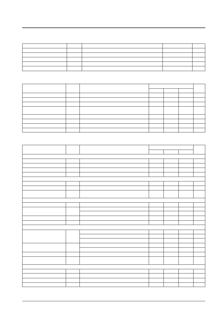
LC75374E
Parameter
Symbol
Conditions
Ratings
Unit
Maximum supply voltage
V
DD
max
V
DD
11
V
Maximum input voltage
V
IN
max
CL, DI, CE
V
SS
≠ 0.3 to V
DD
+ 0.3
V
Allowable power dissipation
Pd max
When Ta
85∞C and mounted on a printed circuit board
720
mW
Operating temperature
Topr
≠40 to +85
∞C
Storage temperature
Tstg
≠50 to +125
∞C
Specifications
Absolute Maximum Ratings
at Ta = 25∞C, V
SS
= 0 V
Parameter
Symbol
Conditions
Ratings
Unit
min
typ
max
Supply voltage
V
DD
V
DD
7.5
9.7
V
High-level input voltage
V
IH
CL, DI, CE
4.0
V
DD
V
Low-level input voltage
V
IL
CL, DI, CE
V
SS
1.0
V
Input voltage amplitude
V
IN
CL, DI, CE, LVRIN, RVRIN, L1 to L4, R1 to R4, LFIN,
V
SS
V
DD
Vp-p
RFIN, LSIN, RSIN
Input pulse width
t
W
CL
1
µs
Setup time
t
setup
CL, DI, CE
1
µs
Hold time
t
hold
CL, DI, CE
1
µs
Operating frequency
fopg
CL
500
kHz
Allowable Operating Ranges
at Ta = ≠40 to +85∞C, V
SS
= 0 V
Parameter
Symbol
Conditions
Ratings
Unit
min
typ
max
[Input Block]
Maximum input gain
Gin max
+18.75
dB
Step resolution
Gstep
+1.25
dB
Output load resistance
R
L
10
k
Output impedance
R
O
LSEL0, RSEL0 : R
L
= 10 k
, f = 1 kHz, V
IN
= 1 Vrms
46
[Output Block]
Maximum output gain
Gout max
+8.5
dB
Output load resistance
R
L
10
k
Output impedance
R
O
LFOUT, LROUT, RFOUT, RROUT : R
L
= 10 k
,
35
f = 1 kHz, V
IN
= 1 Vrms
[Volume Control Block]
Step resolution
ATstep
1
dB
Step error
ATerr
STEP = 0 dB to ≠20 dB
≠1
0
+1
dB
STEP = ≠20 dB to ≠50 dB
≠3
0
+3
dB
Output load resistance
R
L
10
k
Output impedance
R
O
LTOUT, RTOUT : R
L
= 10 k
, f = 1 kHz, V
IN
= 1 Vrms
46
[Fader Volume Control Block]
STEP = 0 dB to ≠20 dB
2
dB
Step resolution
ATstep
STEP = ≠20 dB to ≠25 dB
5
dB
STEP = ≠25 dB to ≠45 dB
10
dB
Step error
ATerr
STEP = 0 dB to ≠45 dB
≠2
0
+2
dB
STEP = ≠45 dB to ≠60 dB
≠3
0
+3
dB
Output load resistance
R
L
10
k
Output impedance
R
O
LFOUT, LROUT, RFOUT, RROUT : R
L
= 10 k
,
46
f = 1 kHz, V
IN
= 1 Vrms
[Bass and Treble Control Block]
Bass control range
Gbass
Max. Boost/Cut
±8
±11.9
±13
dB
Treble control range
Gtre
Max. Boost/Cut
±8
±11.9
±13
dB
Output load resistance
R
L
10
k
Output impedance
R
O
LTOUT, RTOUT : R
L
= 10 k
, f =1 k
, V
IN
= 1 Vrms
46
Electrical Characteristics
at Ta = 25∞C, V
DD
= 8 V, V
SS
= 0 V
Continued on next page.

No. 5835-3/17
LC75374E
Continued from preceding page.
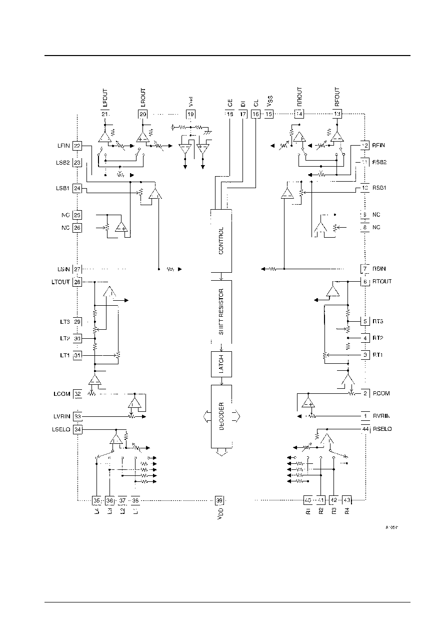
Pin Assignment
Parameter
Symbol
Conditions
Ratings
Unit
min
typ
max
[Super-Bass Block] (T type)
Control range
Crange
Max. Boost
+20
dB
Step resolution
ATstep
+2.0
dB
Output load resistance
R
L
10
k
Output impedance
R
O
LSB2, RSB2 : R
L
= 10 k
, f = 1 kHz, V
IN
= 1 Vrms
70
[Overall]
Total harmonic distortion
THD
V
IN
= 1 Vrms, f = 1 kHz, All controls flat overall
0.003
0.01
%
Crosstalk
CT
V
IN
= 1 Vrms, f = 1 kHz, All controls flat overall, Rg = 1 k
80.5
dB
Output at maximum attenuation
Vo min
V
IN
= 1 Vrms, f = 1 kHz, Main volume setting: ≠
≠80
dB
Output noise voltage
V
N
1
All controls flat overall, (IHF-A), Rg = 1 k
8
µV
V
N
2
All controls flat overall, (DIN-AUDIO), Rg = 1 k
10
µV
High-level input voltage
I
IH
CL, DI, CE, V
IN
= 8 V
10
µA
Low-level input voltage
I
IL
CL, DI, CE, V
IN
= 0 V
≠10
µA
Electrical Characteristics
at Ta = 25∞C, V
DD
= 8 V, V
SS
= 0 V
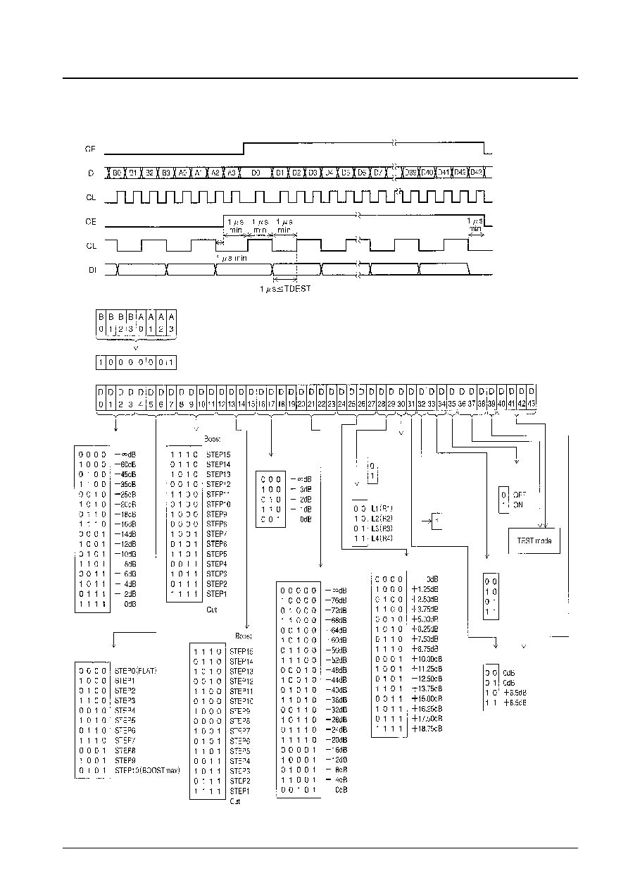
Control System Timing and Data Format
Applications must input the stipulated serial data to the CE, CL, and DI pins to control the LC75374E. The data consists
of a total of 52 bits, of which 8 bits are address and 44 bits are data.
Note: Bits D36 to D38 and bits D40 to D43 are IC test
data. Applications must set all these bits to 0.
No. 5835-5/17
LC75374E
Address code
Fader step control
Bass control
1dB step control
Fader rear/front
control
Input switching control
Input muting
control
Channel selection
Super bass/super treble control
Treble control
4dB step control
Input gain control
Output gain control
Rear
Front
Initial setting
Lch
Rch
Left and right at
the same time