 | –≠–ª–µ–∫—Ç—Ä–æ–Ω–Ω—ã–π –∫–æ–º–ø–æ–Ω–µ–Ω—Ç: LC75383E | –°–∫–∞—á–∞—Ç—å:  PDF PDF  ZIP ZIP |
Ordering number : EN5002A
N2095HA (OT)/62895HA (OT) No. 5002-1/17
Overview
The LC75383E is an electronic volume control that
provides volume, balance, fader, bass/treble, input
switching and input level controls. The LC75383E
supports all these functions while requiring a minimum
number of external components.
Features
∑ Volume: 0 dB to ≠79 dB (in 1 dB steps) and ≠
;
81 positions.
A balance function can be implemented using the
LC75383E independent left and right volume control
functions.
∑ Fader: The rear channels or the front channels can be
attenuated over 16 positions: from 0 dB to ≠20 dB in
2 dB steps, from ≠20 dB to ≠25 dB in one 5 dB step,
from ≠25 dB to ≠45 dB in 10 dB steps, ≠60 dB, and ≠
for a total of 16 positions.
∑ Bass/treble: The LC75383E supports 21 position bass
and treble controls using external capacitors.
∑ Input selector: The LC75383E can select one of four
L/R inputs. The selected input signal can be amplified
from 0 dB to +18 dB in 6 dB steps.
∑ Built-in operational amplifiers mean that few external
components are required.
∑ Silicon gate process for minimal switching noise.
∑ All controls can be set from serial input data (CCB).
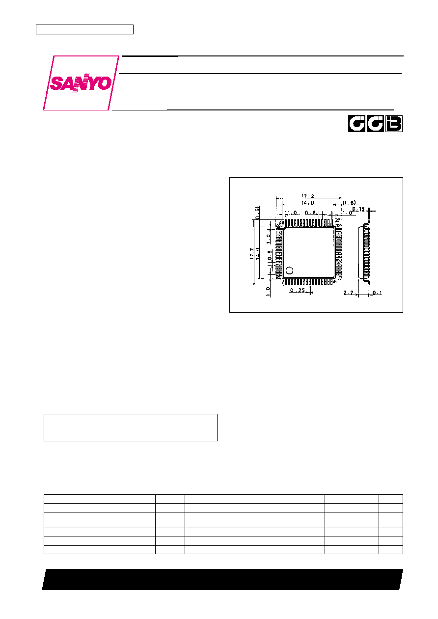
Package Dimensions
unit: mm
3159-QFP64E
SANYO: QIP64E
[LC75383E]
LC75383E
SANYO Electric Co.,Ltd. Semiconductor Bussiness Headquarters
TOKYO OFFICE Tokyo Bldg., 1-10, 1 Chome, Ueno, Taito-ku, TOKYO, 110-8534 JAPAN
Electronic Volume Control
for Car Audio Systems
CMOS LSI
∑ CCB is a trademark of SANYO ELECTRIC CO., LTD.
∑ CCB is SANYO's original bus format and all the bus
addresses are controlled by SANYO.
Specifications
Absolute Maximum Ratings
at Ta = 25∞C, V
SS
= 0 V
Parameter
Symbol
Conditions
Ratings
Unit
Maximum supply voltage
V
DD
max
V
DD
12
V
Maximum input voltage
V
IN
max
CL, DI, CE, LTIN, RTIN, L10dBIN, R10dBIN, L1dBIN,
V
SS
≠ 0.3 to V
DD
+ 0.3
V
R1dBIN, LFIN, RFIN, L1 to L4, R1 to R4
Allowable power dissipation
Pd max
Ta
85∞C
310
mW
Operating temperature
Topr
≠40 to +85
∞C
Storage temperature
Tstg
≠50 to +125
∞C
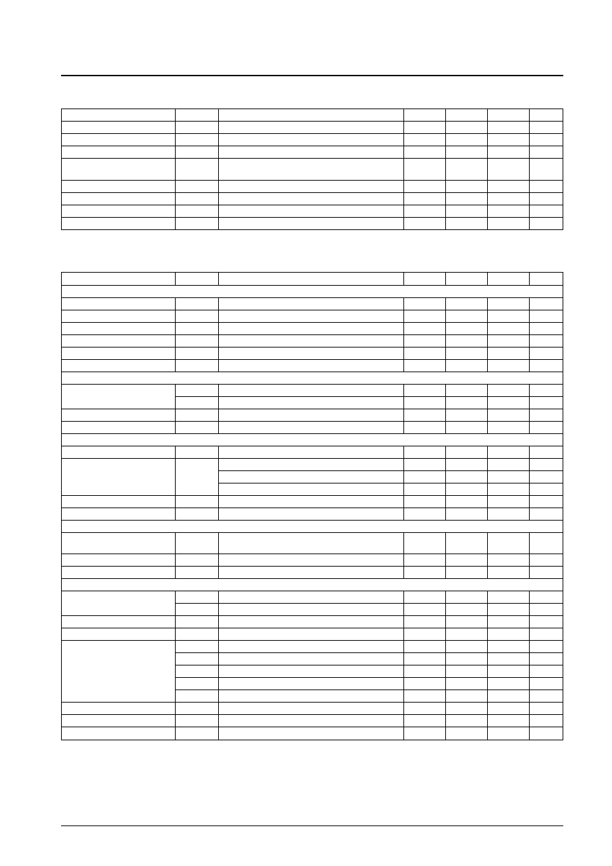
Allowable Operating Ranges
at Ta = 25∞C, V
SS
= 0 V
Electrical Characteristics
at Ta = 25∞C, V
DD
= 9 V, V
SS
= 0 V
No. 5002-2/17
LC75383E
Parameter
Symbol
Conditions
min
typ
max
Unit
Supply voltage
V
DD
V
DD
6.0
11.0
V
Input high level voltage
V
IH
CL, DI, CE
4.0
V
DD
V
Input low level voltage
V
IL
CL, DI, CE
V
SS
1.0
V
Input voltage amplitude
V
IN
LTIN, RTIN, L10dBIN, R10dBIN, L1dBIN, R1dBIN,
V
SS
V
DD
Vp-p
LFIN, RFIN, L1 to L4, R1 to R4
Input pulse width
t
¯W
CL
1
µs
Setup time
t
SETUP
CL, DI, CE
1
µs
Hold time
t
HOLD
CL, DI, CE
1
µs
Operating frequency
fopg
CL
500
kHz
Parameter
Symbol
Conditions
min
typ
max
Unit
[Input Block]
Input resistance
Rin
L1, L2, L3, L4, R1, R2, R3, R4
1
M
Clipping level
Vcl
LSELO, RSELO: THD = 1.0%
2.35
Vrms
Output load resistance
R
L
LSELO, RSELO
10
k
Minimum input gain
Gin min
≠2
0
+2
dB
Maximum input gain
Gin max
+16.0
+18.0
+20.0
dB
Step resolution
Gstep
+6.0
dB
[Volume Block]
Input resistance
Rv10
L10dBIN, R10dBIN: 10 dB steps
21
35
49
k
Rv1
L1dBIN, R1dBIN: 1 dB steps
6
10
14
k
Step resolution
ATstep
1
dB
Step error
ATerr
Step = 0 to ≠40 dB, ≠40 to ≠60 dB
≠1
0
+1
dB
[Fader Volume Block]
Input resistance
Rfed
LFIN, RFIN
12
20
28
k
Step = 0 to ≠20 dB
2
dB
Step resolution
ATstep
Step = ≠20 to ≠25 dB
5
dB
Step = ≠25 to ≠45 dB
10
dB
Step error
ATerr
Step = 0 to ≠40 dB, ≠40 to ≠60 dB
≠2
0
+2
dB
Output load resistance
R
L
LFOUT, LROUT, RFOUT, RROUT
10
k
[Bass/Treble Control Block]
Control range
Gbass
Max. boost/cut
±15
±17
±19
dB
Gtre
Step resolution
Bstep
0.7
1.7
2.7
dB
Internal feedback resistance
Rfeed
46
76
107
k
[Overall]
Total harmonic distortion
THD (1)
V
IN
= 300 mVrms, f = 1 kHz, all controls flat overall
0.005
0.01
%
THD (2)
V
IN
= 300 mVrms, f = 20 kHz, all controls flat overall
0.008
0.02
%
Crosstalk
CT
V
IN
= 1 Vrms, f = 1 kHz, all controls flat overall, Rg = 1 k
60
84.5
dB
Maximum attenuation
Vo min
V
IN
= 1 Vrms, f = 1 kHz, main volume at ≠
≠65
≠80
dB
V
N
(1)
All controls flat overall (IHF-A), Rg = 1 k
5.2
12
µV
V
N
(2)
All controls flat overall (DIN-AUDIO), Rg = 1 k
7.2
16
µV
Output noise voltage
V
N
(3)
All controls flat overall (NO-FILTER), Rg = 1 k
9.2
20
µV
V
N
(4)
Gv = +18 dB (IHF-A), Rg = 1 k
23
50
µV
V
N
(5)
Bass = max. boost, treble = max. boost (IHF-A), Rg = 1 k
48
120
µV
Current drain
I
DD
V
DD
≠ V
SS
= 11 V
28
33
mA
Input high level current
I
IH
CL, DI, CE, V
IN
= 9 V
10
µA
Input low level current
I
IL
CL, DI, CE, V
IN
= 0 V
≠10
µA
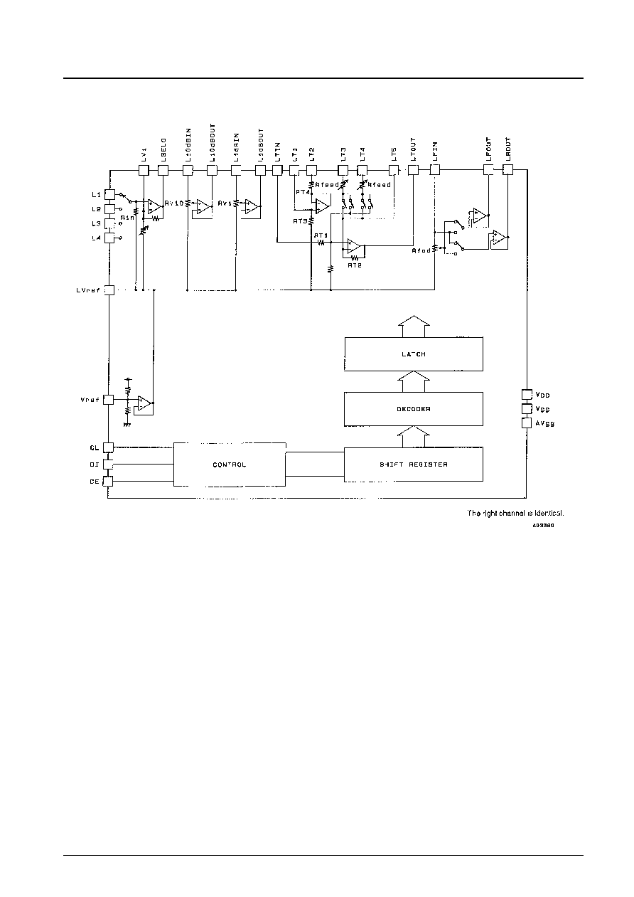
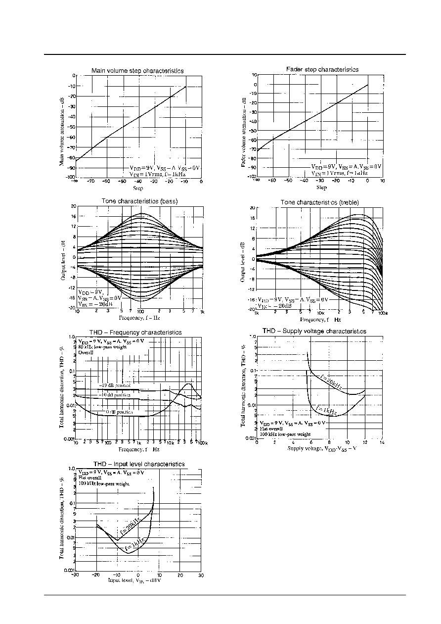
Equivalent Circuit Block Diagram
No. 5002-3/17
LC75383E
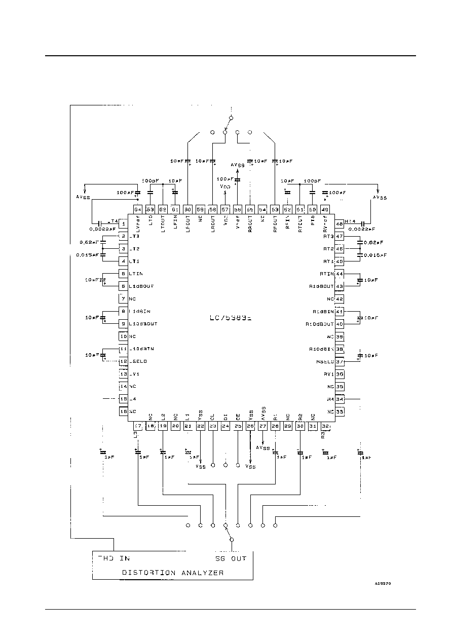
Electrical Characteristics Test Circuits
1. Total Harmonic Distortion
No. 5002-4/17
LC75383E
2. Output Noise Voltage
No. 5002-5/17
LC75383E
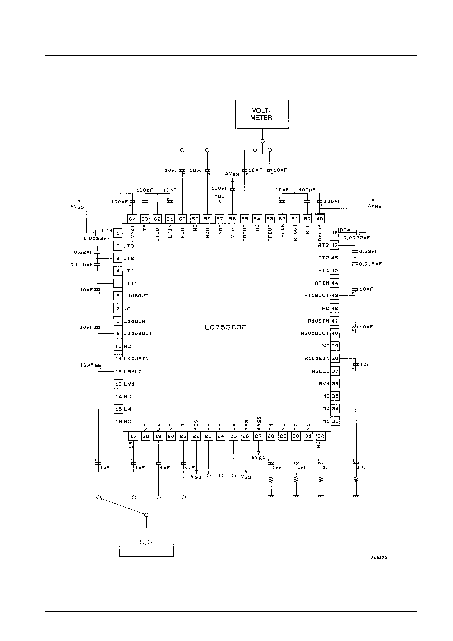
3. Crosstalk
No. 5002-6/17
LC75383E
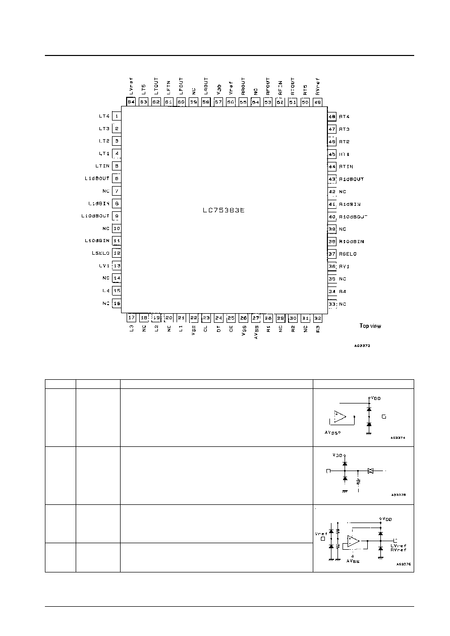
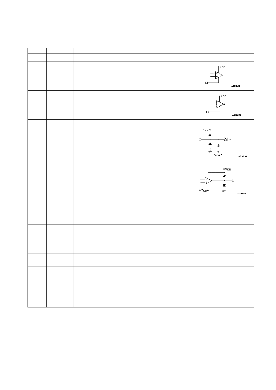
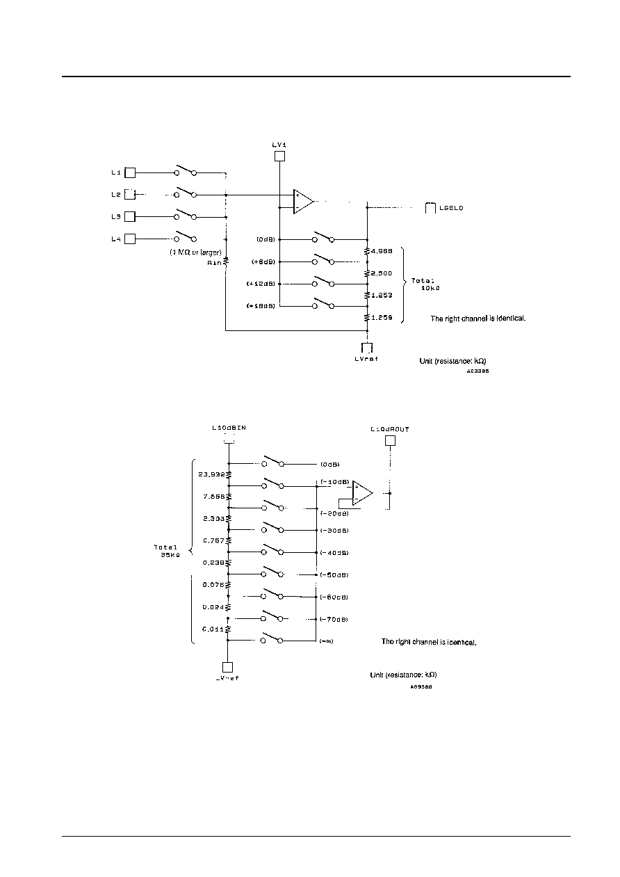
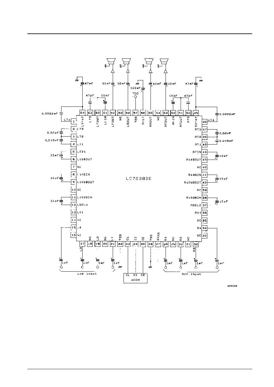
Pin Assignment
Pin Functions
No. 5002-7/17
LC75383E
Pin No.
Symbol
Function
Note
58
60
55
53
61
52
64
49
56
LROUT
LFOUT
RROUT
RFOUT
LFIN
RFIN
LVref
RVref
Vref
Fader block outputs. Only the front or rear channels are attenuated. The left
and right attenuations are identical.
Since these are operational amplifier outputs, the output is low impedance.
Fader block inputs.
Must be driven by low impedance circuits.
Common connections for the main volume, fader block, tone block and gain
control block.
Capacitors of about 100 µF must be inserted between Vref and AV
SS
(V
SS
) to
reduce power supply ripple in the V
DD
/2 voltage generation block.
Continued on next page.
Continued from preceding page.
No. 5002-8/17
LC75383E
Pin No.
Symbol
Function
Note
6
43
8
41
9
40
11
38
62
51
4
3
2
45
46
47
1
48
63
50
5
44
L1dBOUT
R1dBOUT
L1dBIN
R1dBIN
L10dBOUT
R10dBOUT
L10dBIN
R10dBIN
LTOUT
RTOUT
LT1
LT2
LT3
RT1
RT2
RT3
LT4
RT4
LT5
RT5
LTIN
RTIN
Main volume 1 dB step attenuator outputs
Main volume 1 dB step attenuator inputs
Must be driven by low impedance circuits.
Main volume 10 dB step attenuator outputs
Main volume 10 dB step attenuator inputs
Must be driven by low impedance circuits.
Tone control outputs
Connections for the capacitors that form the low frequency (bass) tone control
filters
Low frequency compensation capacitors must be connected between T1 and
T2 and between T2 and T3.
Connections for the capacitors that form the high frequency (treble) tone control
filters
High frequency compensation capacitors must be connected between the T4
pins and Vref.
Inverting inputs for the operational amplifiers that form the tone control circuit
filters
Unnecessary frequencies can be excluded by inserting capacitors of desired
values between the T5 and TOUT pin pairs.
Tone control circuit inputs
Must be driven by low impedance circuits.
Continued on next page.
Continued from preceding page.
No. 5002-9/17
LC75383E
Pin No.
Symbol
Function
Note
57
27
22, 26
21
19
17
15
28
30
32
34
12
37
25
24
23
13
36
7, 10,
14, 16,
18, 20,
29, 31,
33, 35,
39, 42,
54, 59
V
DD
A. V
SS
V
SS
L1
L2
L3
L4
R1
R2
R3
R4
LSELO
RSELO
CE
DI
CL
LV1
RV1
NC
Power supply
Ground for internal operational amplifiers
Ground for the internal logic system
Audio signal inputs
Input selector outputs
Chip enable. Data is written to the internal latch when this pin goes from high to
low. The analog switches operate at that point also. Data transfer is enabled
when this pin is high.
Serial data and clock pins for IC control
Test pins. These pins must be left open.
No connection pins. These pins must be left open or tied to V
SS
.
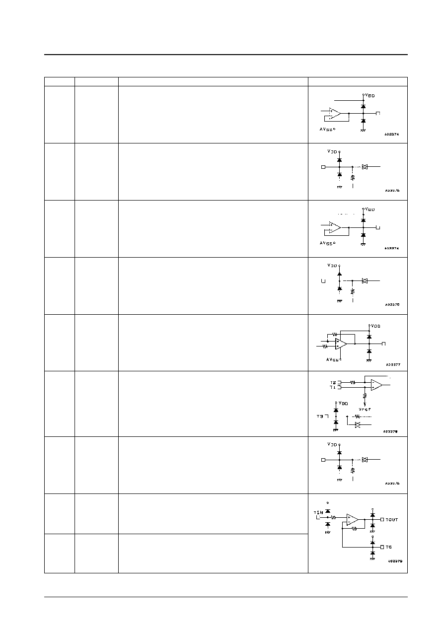
Equivalent Circuit Details
Input Block Equivalent Circuit
10 dB Step Volume Control Equivalent Circuit
No. 5002-10/17
LC75383E
1 dB Step Volume Control Equivalent Circuit
Tone Block Equivalent Circuit
No. 5002-11/17
LC75383E
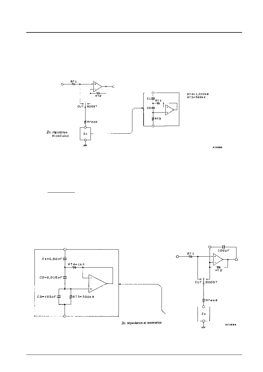
Sample Calculation for the Tone Block External Capacitors
The external capacitors used with the LC75383E are the structural components in semiconductor inductors, i.e.,
simulated inductors. Here we present the equivalent circuit and the formulas required to acquire the desired center
frequency.
1. Semiconductor inductor equivalent circuit
2. Sample calculation
Specifications: 1) Center frequency: Fo = 100 Hz
2) Q at maximum boost: Q
max
= 1.05
∑ Derive the sharpness, Qo, of the semiconductor inductor itself
Qo =
◊
Q
max
2.6481
∑ Calculate C1
C1 = 1/2
FoRT4Qo
0.60 (µF)
∑ Calculate C2
C2 =Qo/2
FoRT3
0.014 (µF)
Note: See the tone block equivalent circuit for the internal resistance.
Technique for Reducing Noise in the Tone Circuit Output
The output noise can be improved by about 6 dB by providing an external impedance at resonance of Zo and adding
the capacitor C3 with a value of about 100 pF. An even larger noise reduction effect can be acquired by using a low
noise operational amplifier in the external circuit.
(RT4 + Rfeed)
RT4
No. 5002-12/17
LC75383E
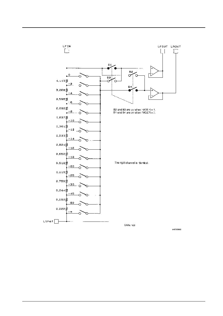
Fader Volume Control Equivalent Circuit
When the main volume 1dBSTEP setting is set to the data value for ≠
, S1 and S2 will be open and at the same time S3
and S4 will be on.
No. 5002-13/17
LC75383E
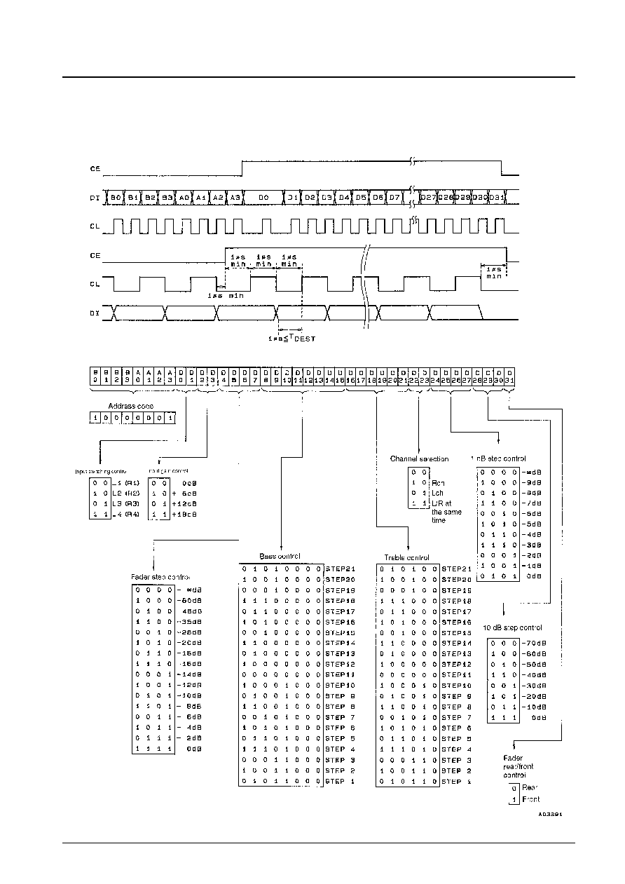
Control System Timing and Data Format
The LC75383E is controlled by inputting the stipulated serial data to the CE, CL and DI pins. The data structure consists
of a total of 40 bits, of which 8 bits are address and 32 bits are setting data.
No. 5002-14/17
LC75383E
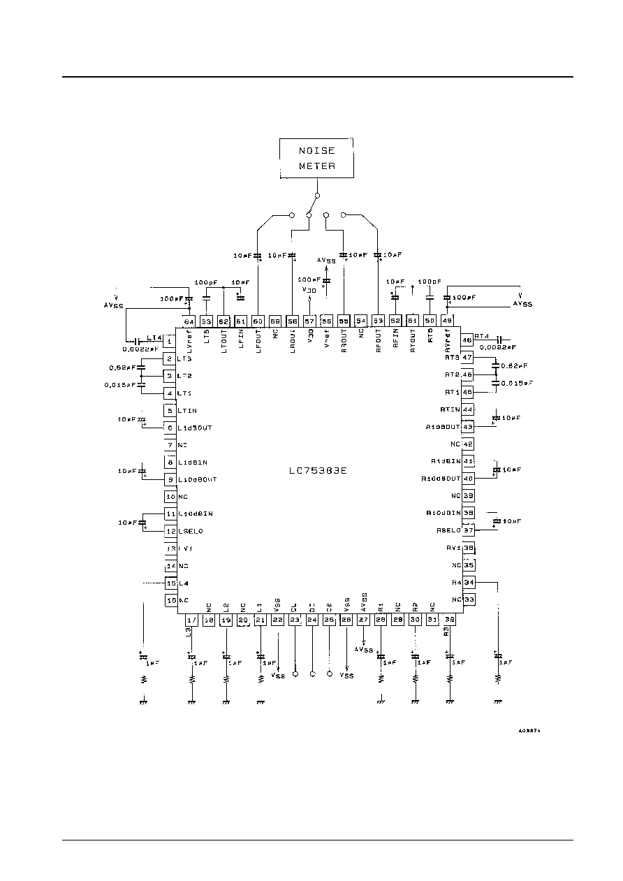
Sample Application Circuit
Usage Notes
1. The states of the internal analog switches are undefined when power is first applied. Muting should be applied
externally until control data has been transferred and stored.
2. The signal lines for the CL, DI and CE pins should either be covered by the pattern ground or be formed from
shielded cable to prevent the high-frequency digital signals transmitted over these lines from entering the analog
system.
No. 5002-15/17
LC75383E
No. 5002-16/17
LC75383E

No. 5002-17/17
LC75383E
This catalog provides information as of February, 1997. Specifications and information herein are subject to
change without notice.
s
No products described or contained herein are intended for use in surgical implants, life-support systems, aerospace
equipment, nuclear power control systems, vehicles, disaster/crime-prevention equipment and the like, the failure of
which may directly or indirectly cause injury, death or property loss.
s
Anyone purchasing any products described or contained herein for an above-mentioned use shall:
Accept full responsibility and indemnify and defend SANYO ELECTRIC CO., LTD., its affiliates, subsidiaries and
distributors and all their officers and employees, jointly and severally, against any and all claims and litigation and all
damages, cost and expenses associated with such use:
Not impose any responsibility for any fault or negligence which may be cited in any such claim or litigation on
SANYO ELECTRIC CO., LTD., its affiliates, subsidiaries and distributors or any of their officers and employees
jointly or severally.
s
Information (including circuit diagrams and circuit parameters) herein is for example only; it is not guaranteed for
volume production. SANYO believes information herein is accurate and reliable, but no guarantees are made or implied
regarding its use or any infringements of intellectual property rights or other rights of third parties.