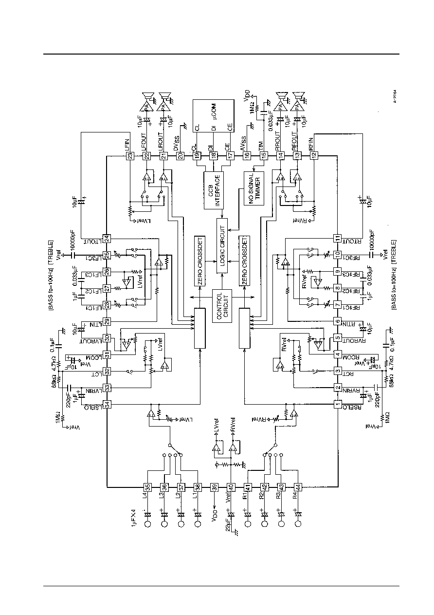
Overview
The LC75385NE-R is an electronic volume and tone
control IC that can implement volume, balance, fader,
bass/treble, loudness, input switching, and input gain
control functions with a minimum number of external
components.
Features
∑ Volume: 81 positions: from 0 dB to ≠79 dB in 1-dB steps
and ≠
.
A balance function can be implemented by
controlling the left and right volume settings
independently.
∑ Fader: Either the rear or front outputs can be attenuated
over 16 positions. (16 positions: From 0 dB to
≠2 dB in 1-dB steps, from ≠2 dB to ≠20 dB in
2-dB steps, from ≠20 to ≠30 dB in one 10-dB step,
≠45 dB, ≠60 dB, and ≠
.)
∑ Bass/treble: Control over ±12 dB in 2-dB steps in each
band.
∑ Input gain: The input signal can be amplified by from 0
to +18.75 dB in 1.25 dB steps.
∑ Input switching: One of four signals can be selected for
each of the left and right channels.
∑ Loudness: Taps are output from a 2-dB step volume
control ladder resistor starting at the ≠32-dB
position. A loudness function can be
implemented by attaching external capacitors
and resistors.
∑ On-chip buffer amplifiers minimize the number of
required external components.
∑ Minimal switching noise when no input signals are
present due to fabrication in a silicon gate CMOS
process that minimizes the noise generated by internal
switches.
∑ Use of zero-cross switching circuits for internal switches
minimizes switching noise when signals are present.
∑ Built-in V
DD
/2 reference voltage generator circuit
∑ All controls can be set from serial input data transferred
over a CCB interface.
Package Dimensions
unit: mm
3148-QFP44MA
2.8max
0.8
11.6
0.35
10.0
13.2
1.0
1
11
12
22
23
33
34
44
1.0
1.6
0.8
2.5
0.2
0.1
10.0
13.2
1.0
1.0
1.6
0.8
CMOS IC
41399RM (OT) No.6143-1/22
SANYO: QFP44MA (QIP44MA)
[LC75385NE-R]
SANYO Electric Co.,Ltd. Semiconductor Company
TOKYO OFFICE Tokyo Bldg., 1-10, 1 Chome, Ueno, Taito-ku, TOKYO, 110-8534 JAPAN
Electronic Volume and Tone Control
for Car Stereo Systems
LC75385NE-R
Ordering number : EN6143
∑ CCB is a trademark of SANYO ELECTRIC CO., LTD.
∑ CCB is SANYO's original bus format and all the bus
addresses are controlled by SANYO.
Any and all SANYO products described or contained herein do not have specifications that can handle
applications that require extremely high levels of reliability, such as life-support systems, aircraft's
control systems, or other applications whose failure can be reasonably expected to result in serious
physical and/or material damage. Consult with your SANYO representative nearest you before using
any SANYO products described or contained herein in such applications.
SANYO assumes no responsibility for equipment failures that result from using products at values that
exceed, even momentarily, rated values (such as maximum ratings, operating condition ranges, or other
parameters) listed in products specifications of any and all SANYO products described or contained
herein.
No.6143-3/22
LC75385NE-R
Overall Characteristics
Parameter
Symbol
Conditions
Ratings
Unit
min
typ
max
Total harmonic distortion
THD 1
V
IN
= ≠10 dBV, f = 1 kHz
0.004
%
THD 2
V
IN
= ≠10 dBV, f = 10 kHz
0.006
%
Inter-input crosstalk
CT
V
IN
= 1 Vrms, f = 1 kHz
80
88
dB
Left/right channel crosstalk
CT
V
IN
= 1 Vrms, f = 1 kHz
80
88
dB
Maximum attenuation
V
O
min 1
V
IN
= 1 Vrms, f = 1 kHz
80
88
dB
V
O
min 2
V
IN
= 1 Vrms, f = 1 kHz, INMUTE, with the fader set to ≠
90
95
dB
Output noise voltage
V
N
1
All controls flat, with the IHF-A filter
5
10
µV
V
N
2
All controls flat, with a 20 Hz to 20 kHz bandpass filter
7
15
µV
Current drain
I
DD
33
40
mA
High-level input current
I
IH
CL, DI, CE, V
IN
= 9 V
10
µA
Low-level input current
I
IL
CL, DI, CE, V
IN
= 0 V
≠10
µA
Maximum input voltage
V
CL
THD = 1 %, R
L
= 10 k
, all controls flat, FiN = 1 kHz
2.5
2.9
Vrms
Pin Arrangement
1
RSELO
2
RVRIN
3
RCT
4
RCOM
5
RVROUT
6
RTIN
7
RF1C1
8
RF1C2
9
RF1C3
10
RF3C1
11
12 RFIN
13 RFOUT
14 RROUT
15 TIM
16 AVSS
17 CE
18 DI
19 CL
20 DVSS
21 LROUT
22
23
LFIN
24
LTOUT
25
LF3C1
26
LF1C3
27
LF1C2
28
LF1C1
29
LTIN
30
LVROUT
31
LCOM
32
LCT
33
34
LSELO
35
L4
36
L3
37
L2
38
L1
39
VDD
40
Vref
41
R1
42
R2
43
R3
44
R4
LVRIN
LFOUT
RTOUT
LC75385NE-R
A12263
Top view
Printed circuit board size:
76.1
◊
114.3
◊
1.6 mm
Printed circuit board material:
Fiberglass/epoxy
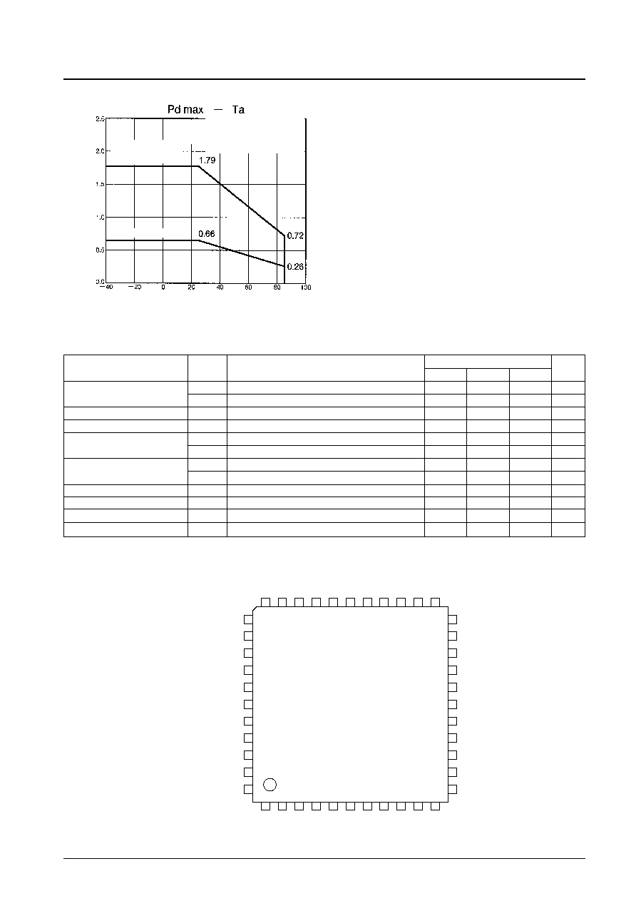
Ambient temperature, Ta (∞C)
Allowable power dissipation, Pdmax (W)
Mounted on the
stipulated printed
circuit board
Independent device
No.6143-5/22
LC75385NE-R
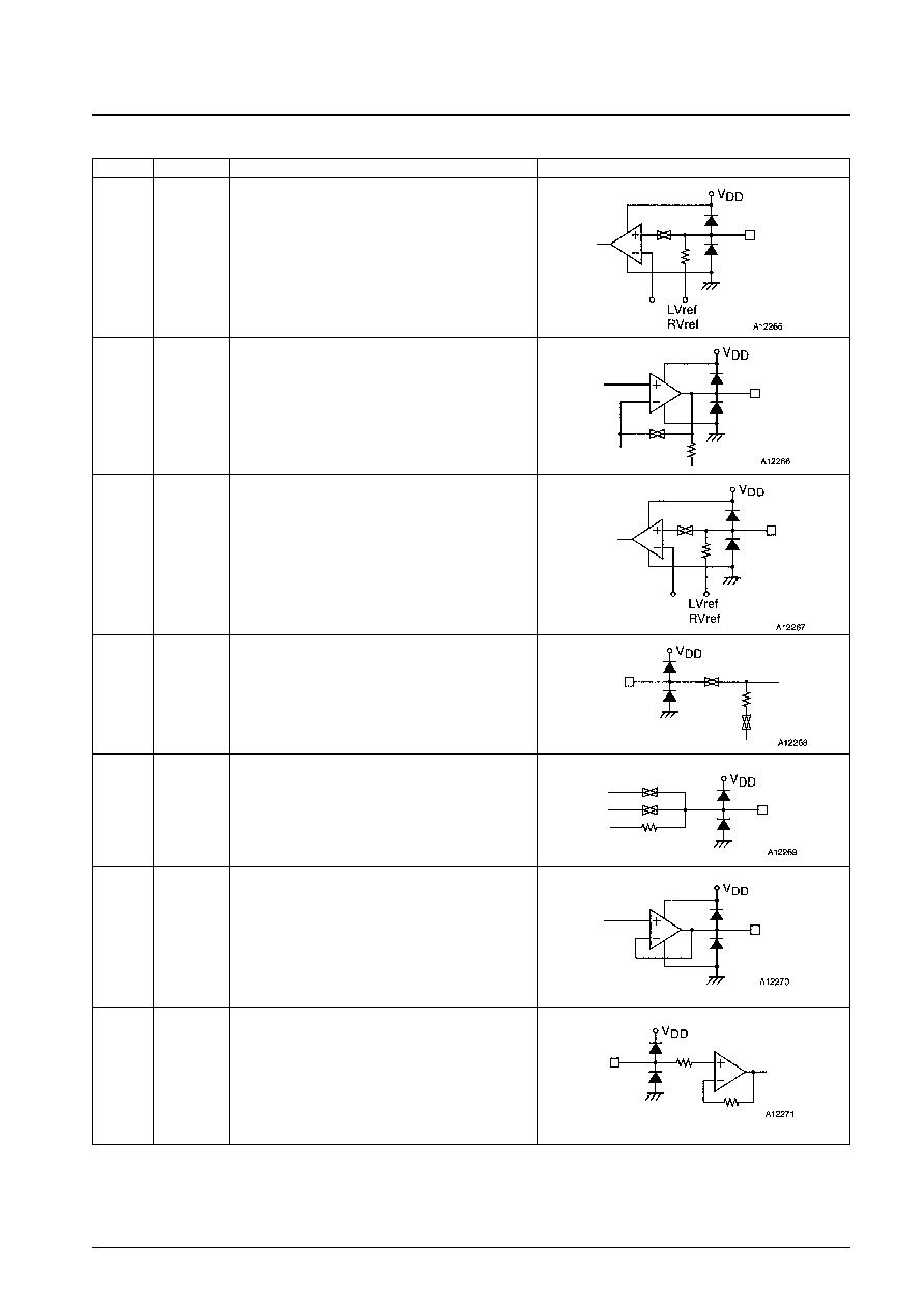
Pin Functions
Pin No.
Pin
Function
Notes
∑ Single end inputs
38
37
36
35
41
42
43
44
L1
L2
L3
L4
R1
R2
R3
R4
∑ Input selector outputs
34
1
LSEL0
RSEL0
∑ Inputs for the 2-dB step volume control
∑ These inputs must be driven from low-impedance circuits.
33
2
LVRIN
RVRIN
∑ Loudness function pins. Connect the high-band
compensation RC circuits between the LCT (RCT) and the
LVRIN (RVRIN) pins and connect the low-band
compensation RC circuits between the LCT (RCT) and Vref.
32
3
LCT
RCT
∑ 2-dB step volume control outputs
∑ To reduce switching noise, each of these pins should be
connected to Vref through a capacitor.
31
4
LCOM
RCOM
∑ Output from the 1-dB step volume control
30
5
LVROUT
RVROUT
∑ Tone control circuit inputs
29
6
LTIN
RTIN
Continued on next page.