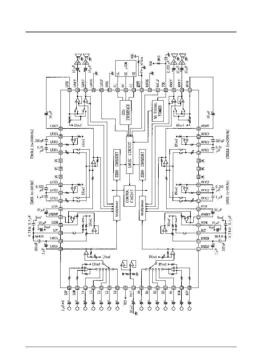
Overview
The LC75386NE is an electronic volume and tone control
IC that can implement a wide range of functions including
volume, balance, fader, bass and treble controls, loudness,
input switching, and input gain control with a minimal
number of external components.
Functions
∑ Volume:
0 to ≠79 dB ( in 1-dB steps) and ≠
for
a total of 81 settings.
A balance function can be implemented
by controlling the left and right channel
volume settings independently.
∑ Fader:
The rear or the front outputs can be
attenuated over 16 settings.
(0 to ≠2 dB in 1-dB steps, ≠2 to ≠20 dB
in 2 dB steps, ≠20 to ≠30 dB in 10-dB
steps, ≠45 dB, -60 dB, and ≠
for a
total of 16 settings.)
∑ Bass and treble: Control over a ±12-dB range in 2-dB
steps in each band.
∑ Input gain:
The input signal can be amplified from
0 to +18.75 dB (in 1.25-dB steps).
∑ Input switching: One of 6 inputs can be selected for
each of the left and right channels.
(Five are single-ended inputs, and one
is a differential input.)
∑ Loudness:
Taps are output from the ≠32-dB
positions of the 2-dB step volume
ladder resistors, and loudness operation
can be implemented by attaching
external capacitors.
Features
∑ On-chip buffer amplifiers minimize the number of
external components required.
∑ The low level of switching noise generated from internal
switches due to fabrication in a CMOS process
minimizes switching noise when no input signals are
present.
∑ The use of built-in zero-cross switching circuits
minimizes switching noise when input signals are
present.
∑ Built-in VDD/2 reference voltage generation circuit
∑ All controls are controlled from CCB serial data input.
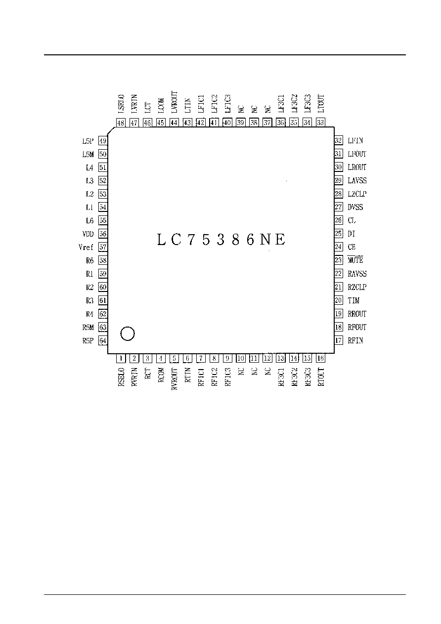
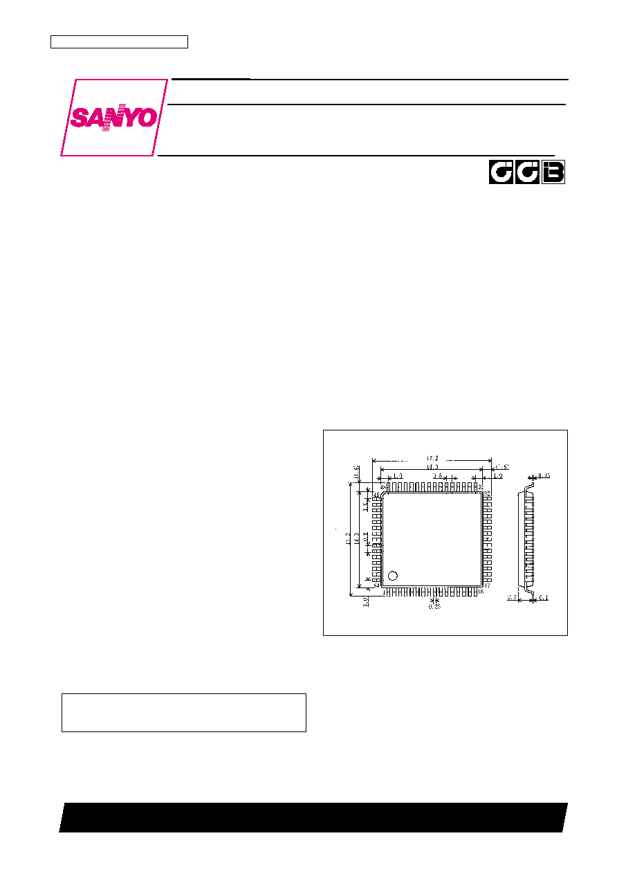
Package Dimensions
unit: mm
3159-QFP64E
CMOS IC
51298RM (OT) No. 5937-1/20
Preliminary
SANYO: QFP64E
[LC75386NE]
SANYO Electric Co.,Ltd. Semiconductor Bussiness Headquarters
TOKYO OFFICE Tokyo Bldg., 1-10, 1 Chome, Ueno, Taito-ku, TOKYO, 110-8534 JAPAN
Electronic Volume and Tone Control
for Car Stereo Systems
LC75386NE
Ordering number : EN
*
5937
∑ CCB is a trademark of SANYO ELECTRIC CO., LTD.
∑ CCB is SANYO's original bus format and all the bus
addresses are controlled by SANYO.

No. 5937-4/20
LC75386NE
Parameter
Symbol
Conditions
Ratings
Unit
Maximum supply voltage
V
DD
max
V
DD
11
V
Maximum input voltage
V
IN
max
All input pins
V
SS
≠ 0.3 to V
DD
+ 0.3
V
Operating temperature
Topr
≠40 to +85
∞C
Storage temperature
Tstg
≠50 to +125
∞C
Specifications
Absolute Maximum Ratings
at Ta = 25∞C, V
SS
= 0 V
Parameter
Symbol
Conditions
Ratings
Unit
min
typ
max
Supply voltage
V
DD
V
DD
6.0
10.5
V
High-level input voltage
V
IH
CL, DI, CE
4.0
V
DD
V
Low-level input voltage
V
IL
CL, DI, CE
V
SS
1.0
V
Input amplitude
V
IN
V
SS
V
DD
Vp-p
Input pulse width
T¯W
CL
1
µs
Setup time
Tsetup
CL, DI, CE
1
µs
Hold time
Thold
CL, DI, CE
1
µs
Operating frequency
fopg
CL
500
kHz
Allowable Operating Ranges
at Ta = 25∞C, V
SS
= 0 V
Parameter
Symbol
Applicable pins
Conditions
Ratings
Unit
min
typ
max
Input resistance
Rin
L1 to L4, L6, R1 to R4, R6
35
50
65
k
Minimum input gain
Ginmin
L1 to L4, L6, R1 to R4, R6
≠1
0
+1
dB
Maximum input gain
Ginmax
+16.5
+18.75
+21
dB
Inter-step setting error
ATerr
±0.6
dB
Left/right balance
BAL
±0.5
dB
Electrical Characteristics
at Ta = 25∞C, V
DD
= 9 V, V
SS
= 0 V
Input Block
Parameter
Symbol
Applicable pins
Conditions
Ratings
Unit
min
typ
max
Input resistance
Rvr
LVRIN, RVRIN, Loudness off
158
226
294
k
Inter-step setting error
ATerr
±0.5
dB
Left/right balance
BAL
±0.5
dB
Volume Control Block
Parameter
Symbol
Applicable pins
Conditions
Ratings
Unit
min
typ
max
Inter-step setting error
ATerr
±1.0
dB
Bass control range
Gbass
max. boost/cut
±9
±12
±15
dB
Treble control range
Gtre
max. boost/cut
±9
±12
±15
dB
Left/right balance
BAL
±0.5
dB
Tone Control Block
No. 5937-5/20
LC75386NE
Parameter
Symbol
Applicable pins
Conditions
Ratings
Unit
min
typ
max
Input resistance
Rfed
LFIN, RFIN
25
50
100
k
0 dB to ≠2 dB
±0.5
dB
Inter-step setting error
ATerr
≠2 dB to ≠20 dB
±1
dB
≠20 dB to ≠30 dB
±2
dB
≠30 dB to ≠60 dB
±3
dB
Left/right balance
BAL
±0.5
dB
Fader Control Block
Parameter
Symbol
Conditions
Ratings
Unit
min
typ
max
Total harmonic distortion
THD1
V
IN
= ≠10 dBV, f = 1 kHz
0.004
0.01
%
THD2
V
IN
= ≠10 dBV, f = 10 kHz
0.006
0.01
%
Inter-input crosstalk
CT
V
IN
= 1 Vrms, f = 1 kHz
80
88
dB
Left/right crosstalk
CT
V
IN
= 1 Vrms, f = 1 kHz
80
88
dB
Maximum attenuation
Vomin1
V
IN
= 1 Vrms, f = 1 kHz
80
88
dB
Vomin2
V
IN
= 1 Vrms, f = 1 kHz, INMUTE, Fader: ≠
90
95
dB
Output noise voltage
VN1
All flat, IHF-A filter
5
10
µV
VN2
All flat, 20 Hz to 20 kHz bandpass filter
7
15
µV
Current drain
I
DD
33
40
mA
High-level input current
I
IH
CL, DI, CE, V
IN
= 9 V
10
µA
Low-level input current
I
IL
CL, DI, CE, V
IN
= 0V
≠10
µA
Maximum input voltage
V
CL
THD = 1%, RL = 10 k
, All flat, f
IN
= 1 kHz
2.5
2.9
Vrms
Overall Characteristics
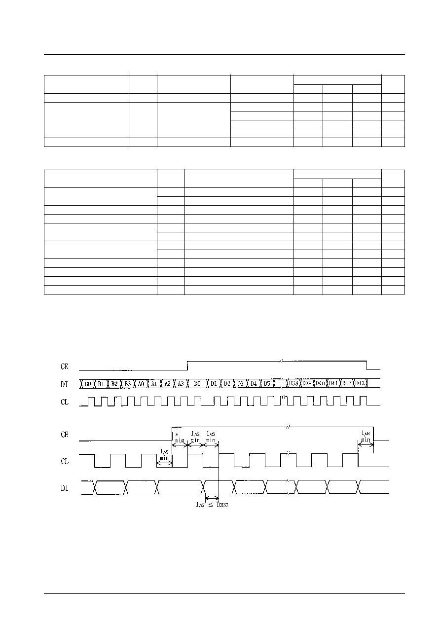
Control System Timing and Data Format
The LC75386NE is controlled by inputting stipulated data serially to the CL, DI, and CE pins. The data consists of a total
of 52 bits, of which 8 bits are the address and 44 bits are the actual control data.
Note
*
: The minimum value is determined by the value of the capacitor connected to the TIM pin (pin 20).
If the value of the capacitor is C
TIM
and the minimum value is T
D
min, then:
T
D
min = 3
◊
10
3
◊
C
TIM
If C
TIM
is 0.033 µF, then:
T
D
min = 3
◊
10
3
◊
0.033
◊
10
≠6
100 µs