Overview
The LC75392 (DIP-30SD) and the LC75392M (MFP-
30S) are electronic volume control ICs that provide input
and output switching, volume, and tone control functions
controlled by data transferred over a serial interface.
Functions
∑ Input and output switching: Four inputs and outputs can
be switched independently.
∑ Volume control: A balance function can be implemented
by controlling the left and right levels independently.
Each channel can be set to 0 to ≠20 dB in 2 dB steps,
≠20 to ≠32 dB in 3 dB steps, ≠32 to ≠52 dB in 4 dB
steps, ≠52 dB to ≠70 dB in 4.5 dB steps, and ≠
.
∑Tone controls: Internal switches are provided to select
between four sets of frequency characteristics. A buffer
function can be implemented using external
components.
Features
Serial data interface: Support for control and
communication in the CCB format.
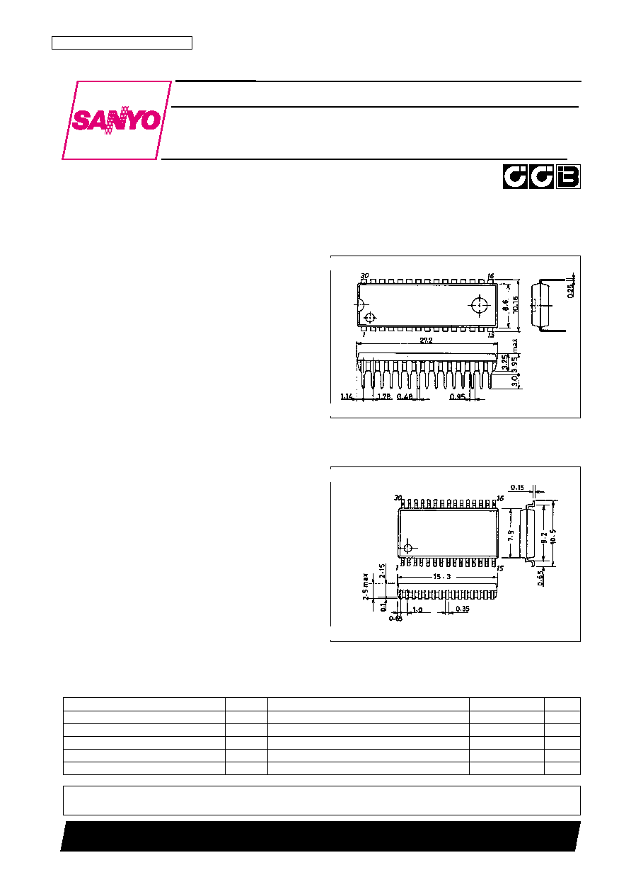
Package Dimensions
unit: mm
3196-DIP30SD
unit: mm
3216-MFP30S
CMOS LSI
Ordering number : EN5681
73097HA(OT) No. 5681-1/12
SANYO: DIP30SD
[LC75392]
SANYO: MFP30S
[LC75392M]
SANYO Electric Co.,Ltd. Semiconductor Bussiness Headquarters
TOKYO OFFICE Tokyo Bldg., 1-10, 1 Chome, Ueno, Taito-ku, TOKYO, 110 JAPAN
Single-Chip Electronic Volume Control System
LC75392, 75392M
∑ CCB is a trademark of SANYO ELECTRIC CO., LTD.
∑ CCB is SANYO's original bus format and all the bus addresses are controlled by SANYO.
Parameter
Symbol
Conditions
Ratings
Unit
Maximum supply voltage
V
DD
max
V
DD
12
V
Maximum input voltage
V
IN
max
CL, DI, CE, L1, L2, L3, L4, R1, R2, R3, R4
V
SS
≠ 0.3 to V
DD
+ 0.3
V
Allowable power dissipation
Pd max
Ta
85∞C
160
mW
Operating temperature
Topr
≠40 to +85
∞C
Storage temperature
Tstg
≠50 to +125
∞C
Specifications
Absolute Maximum Ratings
at Ta = 25∞C, V
SS
= 0 V
No. 5681-2/12
LC75392, 75392M
Parameter
Symbol
Conditions
Ratings
Unit
min
typ
max
Supply voltage
V
DD
V
DD
5.5
11.0
V
Input high-level voltage
V
IH
CL, DI, CE
4.0
V
DD
V
Input low-level voltage
V
IL
CL, DI, CE
V
SS
1.0
V
Input voltage amplitude
V
IN
L1, L2, L3, L4, R1, R2, R3, R4
V
SS
V
DD
Vp-p
Input pulse width
t
¯W
CL
1.0
µs
Setup time
t
setup
CL, DI, CE
1.0
µs
Hold time
t
hold
CL, DI, CE
1.0
µs
Operating frequency
fopg
CL
500
kHz
Allowable Operating Ranges
at Ta = 25∞C, V
SS
= 0 V
Parameter
Symbol
Conditions
Ratings
Unit
min
typ
max
[Input Block]
Input resistance
Rin
L1, L2, L3, L4, R1, R2, R3, R4
500
k
[Overall]
THD1
V
IN
= 100 mV rms, f = 1 kHz,
0.013
%
Total harmonic distortion
overall, buffer mode off, flat state
THD2
V
IN
= 100 mV rms, f = 20 kHz,
0.013
%
overall, buffer mode off, flat state
Crosstalk
CT
V
IN
= 1 V rms, f = 1 kHz, overall, Rg = 1 k
,
81
dB
buffer mode off, flat state
Output at maximum attenuation
V
O
min
V
IN
= 1 V rms, f = 1 kHz, main volume set to
≠80
dB
≠
, buffer mode on
V
N
1
Flat overall (IHF-A), Rg = 1 k
,
15
µV
Output noise voltage
buffer mode off, flat state
V
N
2
Flat overall (DIN-AUDIO), Rg = 1 k
,
22
µV
buffer mode off, flat state
Current drain
I
DD
V
DD
≠ V
SS
= 11 V
7
10
mA
Input high-level current
I
IH
CL, DI, CE, V
IN
= 10 V
10
µA
Input low-level current
I
IL
CL, DI, CE, V
IN
= 0 V
≠10
µA
Electrical Characteristics
at Ta = 25∞C, V
DD
= 10 V, V
SS
= 0 V
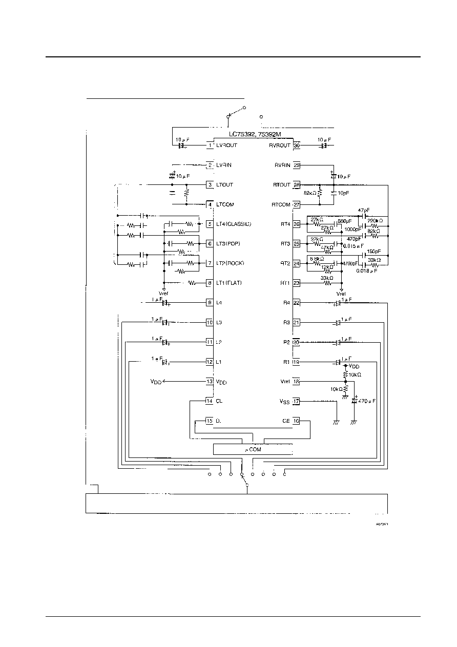
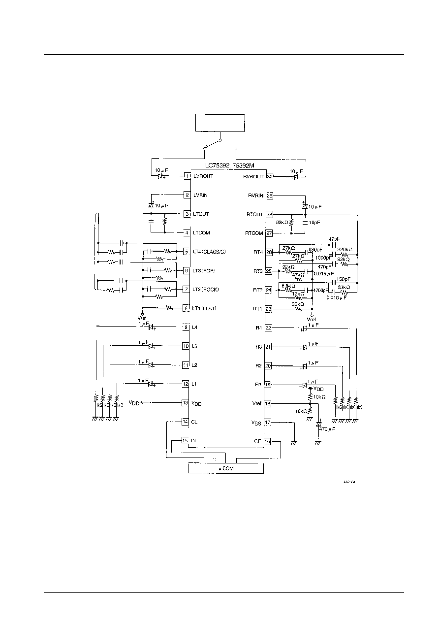
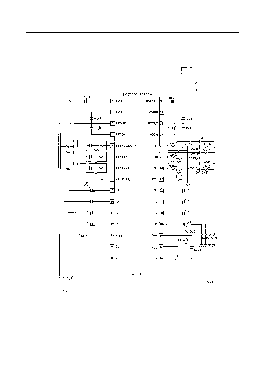
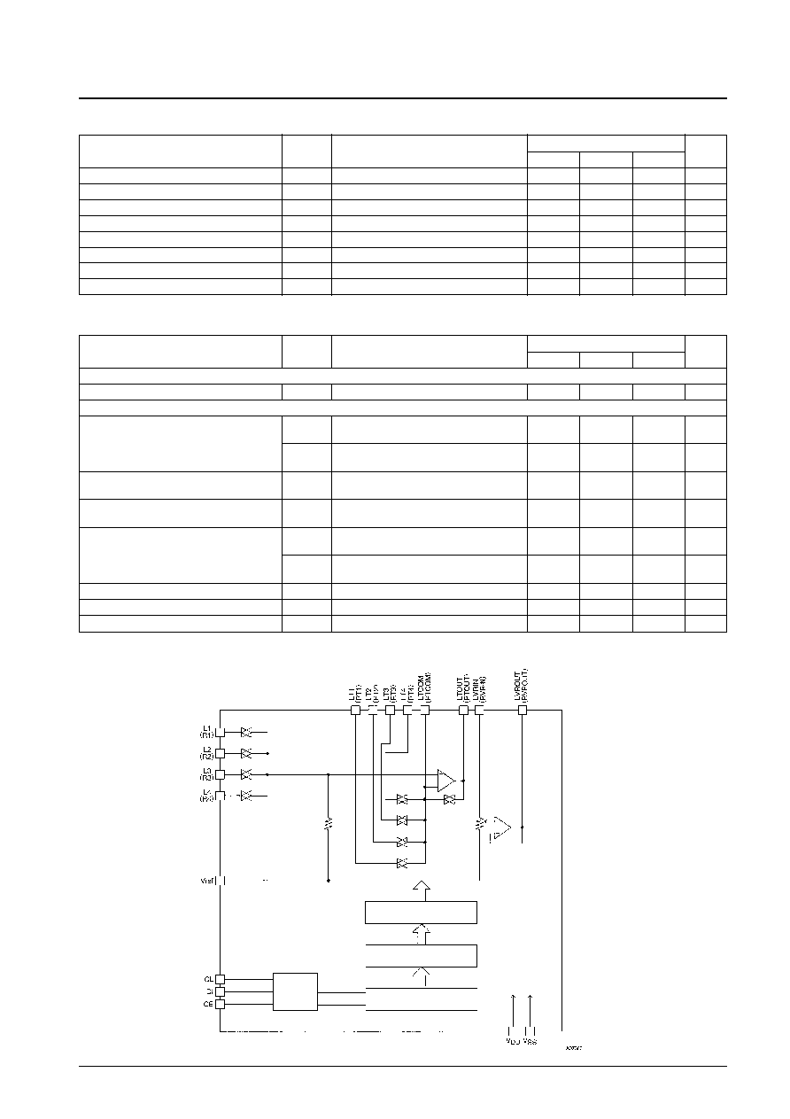
Equivalent Circuit Block Diagram
Latch
Decoder
Shift register
Control