 | –≠–ª–µ–∫—Ç—Ä–æ–Ω–Ω—ã–π –∫–æ–º–ø–æ–Ω–µ–Ω—Ç: LC75397E | –°–∫–∞—á–∞—Ç—å:  PDF PDF  ZIP ZIP |

Ordering number : EN6108
40799RM (OT) No. 6108-1/26
Overview
The LC75397 is an electronic volume control system
providing control over volume, balance, 4-band equalizer,
bass, and input switching based on serial inputs.
Functions
∑ Volume control:
The chip provides 81 levels of volume attenuation: in 1-
dB step between 0 dB and ≠79 dB and ≠
.
This circuit can control a total of 5 independent
channels.
∑ Equalizer:
The chip provides control in 2-dB steps over the range
between +10 dB and ≠10 dB. Three of the four bands
have peaking equalization; the remaining one, shelving
equalization.
∑ Selector:
The left and right channels each offer a choice of six
inputs. The L6 and R6 inputs can be turned on and off
independently. An external constant determines the
amplification for the input signal.
∑ Input gain:
The input signal can be amplified by 0 to +30 dB in 2-
dB steps.
∑ Bass control:
The bass can be controlled over a ±10 dB range in 2-dB
steps.
Features
∑ Built-in buffer amplifiers reduce the number of external
parts required.
∑ Silicon gate CMOS process reduces the noise of built-in
switch.
∑ Built-in analog ground reference voltage generator
circuit
∑ All functions are controlled by serial input data. This IC
supports the CCB standard.
Package Dimensions
unit: mm
3159-QFP64E
14.0
17.2
1.0
1.0
1.6
0.15
0.35
0.1
15.6
0.8
0.8
3.0max
1
16
17
32
33
48
49
64
2.7
14.0
17.2
1.0
1.0
1.6
0.8
SANYO: QFP64E (QIP64E)
[LC75397]
LC75397E
SANYO Electric Co.,Ltd. Semiconductor Company
TOKYO OFFICE Tokyo Bldg., 1-10, 1 Chome, Ueno, Taito-ku, TOKYO, 110-8534 JAPAN
Single Chip Electronic Volume and Tone Control System
CMOS IC
Any and all SANYO products described or contained herein do not have specifications that can handle
applications that require extremely high levels of reliability, such as life-support systems, aircraft's
control systems, or other applications whose failure can be reasonably expected to result in serious
physical and/or material damage. Consult with your SANYO representative nearest you before using
any SANYO products described or contained herein in such applications.
SANYO assumes no responsibility for equipment failures that result from using products at values that
exceed, even momentarily, rated values (such as maximum ratings, operating condition ranges, or other
parameters) listed in products specifications of any and all SANYO products described or contained
herein.
∑ CCB is a trademark of SANYO ELECTRIC CO., LTD.
∑ CCB is SANYO's original bus format and all the bus
addresses are controlled by SANYO.
No. 6108-2/26
LC75397E
Parameter
Symbol
Conditions
Ratings
Unit
Maximum supply voltage
V
DD
max
V
DD
11
V
Maximum input voltage
V
IN
max
CL, DI, CE, L1 to L6, R1 to R6, LTIN, RTIN, LVR1IN,
V
SS
≠ 0.3 to
V
RVR1IN, LVR2IN, RVR2IN, LVR3IN
V
DD
+ 0.3
Allowable power dissipation
Pd max
Ta
75∞C, with PC board
*
1000
mW
Operating temperature
Topr
≠30 to +75
∞C
Storage temperature
Tstg
≠40 to +125
∞C
Specifications
Absolute Maximum Ratings
at Ta = 25∞C, V
SS
= 0 V
Note :
*
Printed circuit board size: 76.1
◊
114.3
◊
1.6 mm, printed circuit board material: glass/Epoxy resin
Parameter
Symbol
Conditions
Ratings
Unit
min
typ
max
Supply voltage
V
DD
V
DD
6.0
10.5
V
Input high level voltage
V
IH
CL, DI, CE
4.0
V
DD
V
Input low level voltage
V
IL
CL, DI, CE
V
SS
1.0
V
Input voltage amplitude
V
IN
CL, DI, CE, L1 to L6, R1 to R6, LTIN, RTIN, LVR1IN,
V
SS
V
DD
Vp-p
RVR1IN, LVR2IN, RVR2IN, LVR3IN
Input pulse width
t
¯W
CL
1.0
µs
Setup time
t
SETUP
CL, DI, CE
1.0
µs
Hold time
t
HOLD
CL, DI, CE
1.0
µs
Operating frequency
fopg
CL
500
kHz
Allowable Operating Ranges
at Ta = ≠ 30 to + 75∞C, V
SS
= 0 V
Parameter
Symbol
Conditions
Ratings
Unit
min
typ
max
[Input block]
Input resistance
Rin
L1 to L6, R1 to R6
50
k
Clipping level
Vcl
LSELO, RSELO: THD = 1.0%
3.00
Vrms
Output load resistance
R
L
LSELO, RSELO
10
k
[Volume control block]
Input resistance
Rin
LVR1IN, RVR1IN, LVR2IN, RVR2IN, LVR3IN
50
k
[Bass control block]
Control range
Geq
Max, boost/cut
±8
±10
±12
dB
Step resolution
Estep
1
2
3
dB
Internal feedback resistance
Rbb1
1.3
k
Rbb2
58
[F1/F2 band equalizer control block]
Control range
Geq
Max. boost/cut
±8
±10
±12
dB
Step resolution
Estep
1
2
3
dB
Internal feedback resistor
Rfeed
31
51.8
73
k
[F3/F4 band equalizer control block]
Control range
Geq
Max. boost/cut
±8
±10
±12
dB
Step resolution
Estep
1
2
3
dB
Internal feedback resistor
Rfeed
17
28
39
k
[Overall characteristics]
Total harmonic distortion
THD
V
IN
= 1 Vrms, f = 1 kHz, with all controls flat overall
0.01
%
Crosstalk
CT
V
IN
= 1 Vrms, f = 1 kHz, with all controls flat overall,
80
dB
Rg = 1 k
Output noise voltage
V
N
1
With all controls flat overall, 80 kHz, L.P.F
10.2
µV
V
N
2
Bass band = +10dB, With all controls overall, 80 kHz, L.P.F
10.6
µV
Output at maximum attenuation
V
O
min
With all controls flat overall
≠90
dB
Current drain
I
DD
V
DD
≠ V
SS
= 10.5 V
58
mA
Input high level current
I
IH
CL, DI, CE, V
IN
= 10.5 V
10
µA
Input low level current
I
IL
CL, DI, CE, V
IN
= 0 V
≠10
µA
Electrical Characteristics
at Ta = 25∞C, V
DD
= 10 V, V
SS
= 0 V
No. 6108-3/26
LC75397E
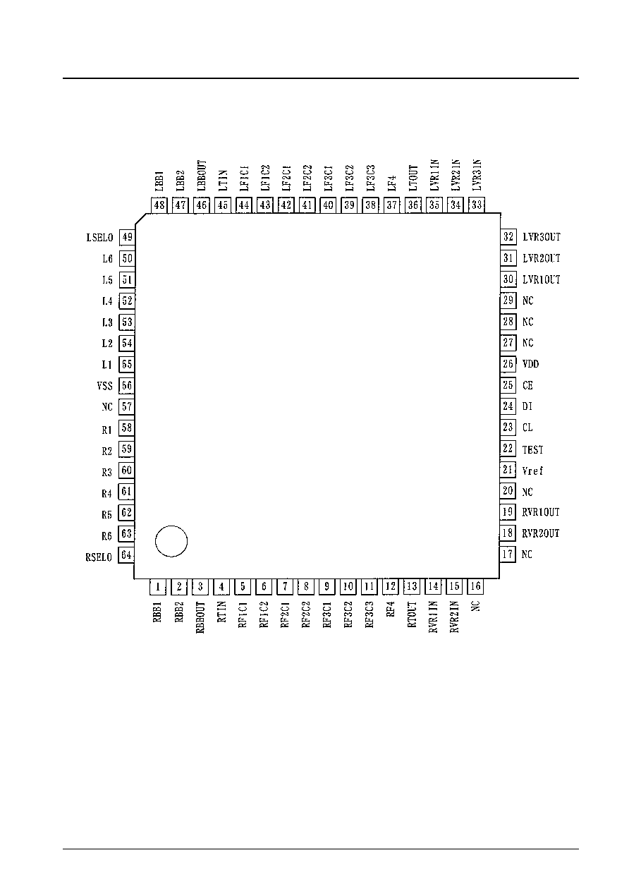
Pin Assignment
L C 7 5 3 9 7 E
Top view
No. 6108-4/26
LC75397E
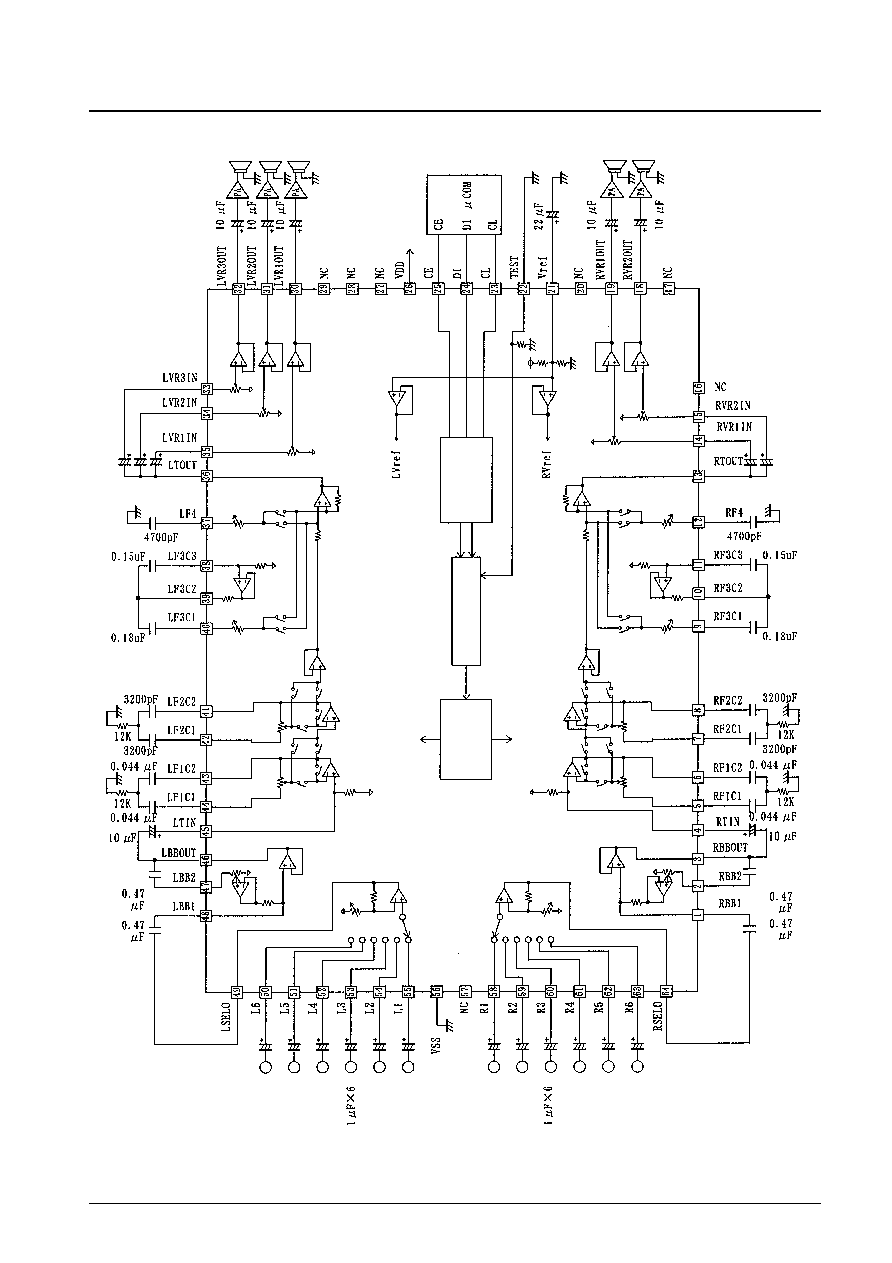
Sample Application Circuit
CCB
interface
Logic circuit
[f0
39 Hz]
[f0
1984 Hz]
[f0
69 Hz]
[fc
20000 Hz]
[f0
39 Hz]
[f0
1984 Hz]
[f0
69 Hz]
[fc
20000 Hz]
[f0
148 Hz]
Control
circuit
LC75397E
[f0
148 Hz]
No. 6108-5/26
LC75397E
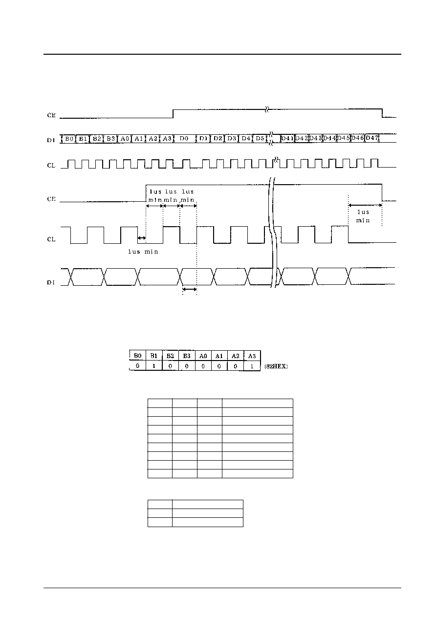
Control System Timing and Data Formats
To control the LC75397E, specified sequences are required to be input through the pins CE, CL, and DI. Each sequence
consists of 48 bits: an 8-bit address followed by 56 bits of data.
1. Address Code (B0 to A3)
This product uses an 8-bit address code, and supports the same specifications as other Sanyo CCB serial bus
products.
Address code (LSB)
2. Control Code Allocations
Input switching control
(L1, L2, L3, L4, L5,
R1, R2, R3, R4, R5)
Input switching control
(L6, R6)
D0
D1
D2
Operation
0
0
0
L1 (R1)
ON
1
0
0
L2 (R2)
ON
0
1
0
L3 (R3)
ON
1
1
0
L4 (R4)
ON
0
0
1
L5 (R5)
OFF
1
0
1
Switch all
OFF
0
1
1
Switch all
OFF
1
1
1
Switch all
OFF
D3
Operation
1
L6 (R6)
OFF
0
L6 (R6)
ON
1us
T DEST