Ordering number : ENN6928
62901RM (OT) No. 6928-1/34
Overview
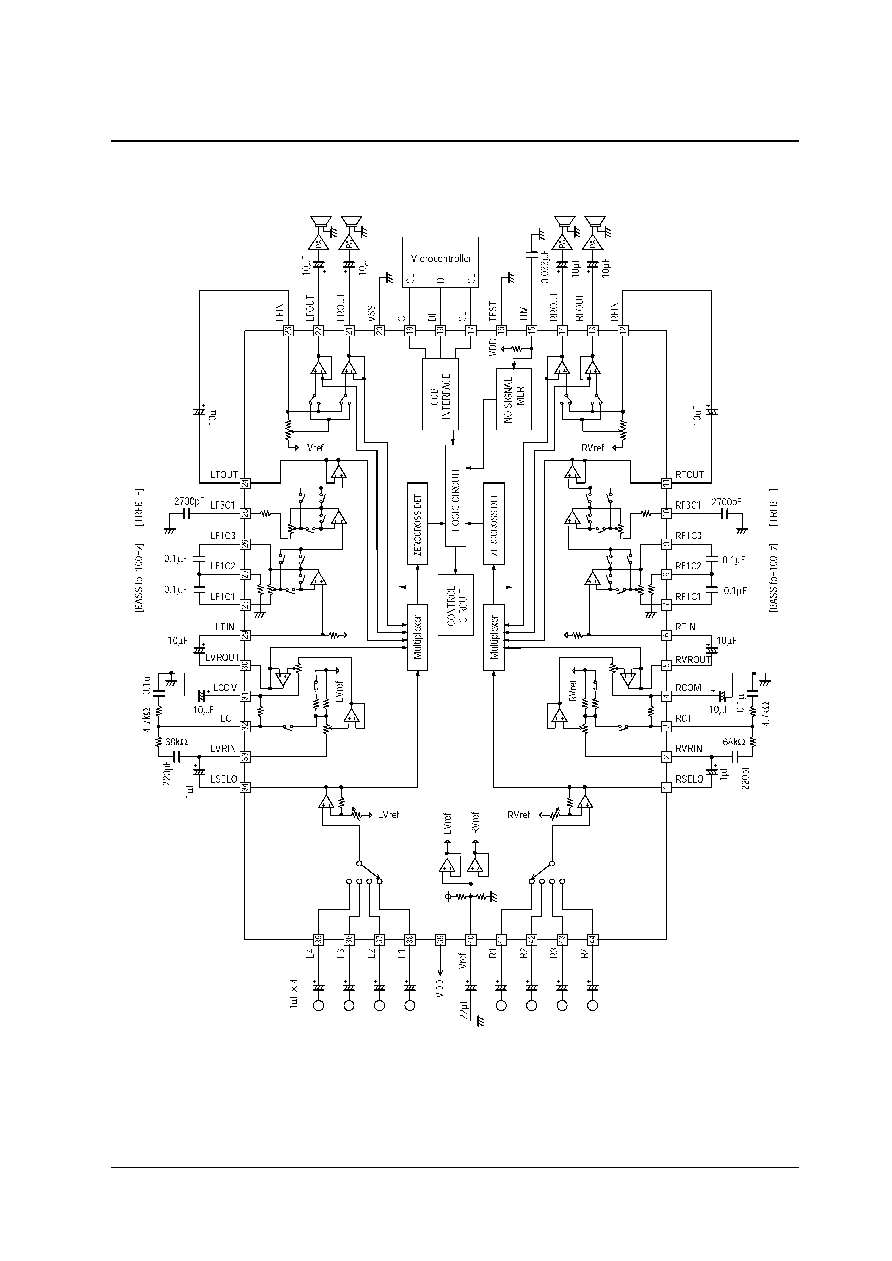
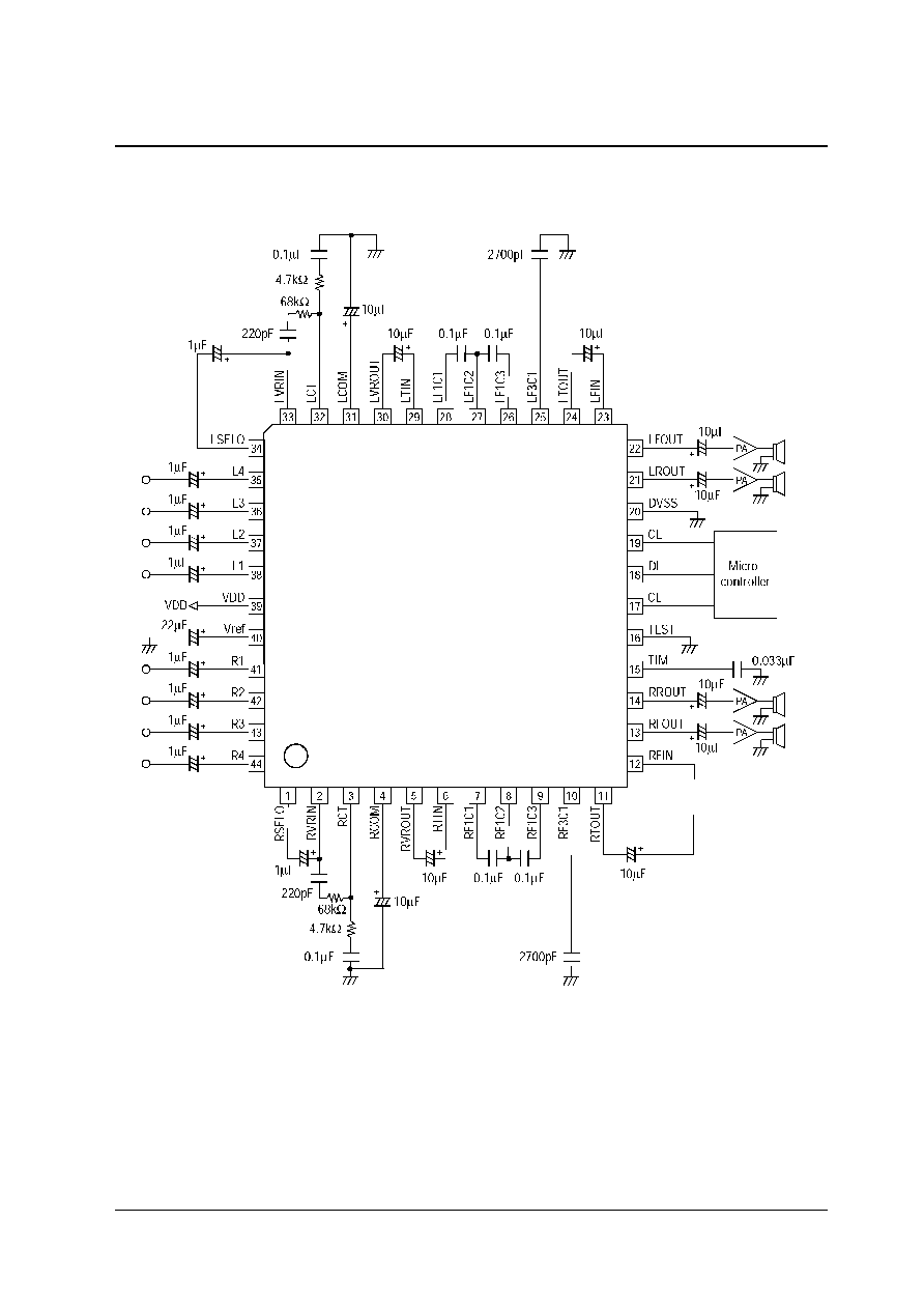
The LC75411ES and 75411WS are electronic volume
controllers that enable control of volume, balance, fader,
bass/treble, loudness, input switching, and input gain
using only a small number of external components.
Functions
∑ Volume: 0 dB to ≠79.5 dB in 0.5-dB steps, and ≠ (161
positions) Balance function with separate L/R
control
∑ Fader: rear output or front output can be attenuated
across 16 positions (in 1-dB steps from 0 dB to
≠2 dB, 2-dB steps from ≠2 dB to 20 dB, 10-dB
steps from ≠20 dB to ≠30 dB, and ≠45 dB,
≠60 dB, ≠ )
∑ Bass/treble: Both bass and treble can be controlled in
1-dB steps from 0 dB to ±6 dB, and in 2-dB
steps from ±8 dB to ±12 dB.
∑ Input gain: 0 dB to +18.75 dB (1.25-dB steps)
amplification is possible for the input signal.
∑ Input switching: four input signals can be selected for
Left and for Right
∑ Loudness: A tap is output from the ≠32 dB position of a
2 dB step volume control resistor ladder.
A loudness function can be implemented by
connecting an external RC circuit.
Features
∑ On-chip buffer amplifier cuts down number of external
components
∑ Low switching noise generated by on-chip switch
through use of silicon gate CMOS process, for low
switching noise when there is no signal
∑ Low switching noise when there is a signal due to use
of on-chip zero-cross switching circuit
∑ On-chip 1/2 VDD reference voltage circuit
∑ Controls performed with serial input (CCB)
LC75411ES, 75411WS
SANYO Electric Co.,Ltd. Semiconductor Company
TOKYO OFFICE Tokyo Bldg., 1-10, 1 Chome, Ueno, Taito-ku, TOKYO, 110-8534 JAPAN
Electronic Volume Controller
for Car Audio Systems
CMOS IC
Any and all SANYO products described or contained herein do not have specifications that can handle
applications that require extremely high levels of reliability, such as life-support systems, aircraft
'
s
control systems, or other applications whose failure can be reasonably expected to result in serious
physical and/or material damage. Consult with your SANYO representative nearest you before using
any SANYO products described or contained herein in such applications.
SANYO assumes no responsibility for equipment failures that result from using products at values that
exceed, even momentarily, rated values (such as maximum ratings, operating condition ranges, or other
parameters) listed in products specifications of any and all SANYO products described or contained
herein.
∑
CCB is a trademark of SANYO ELECTRIC CO., LTD.
∑
CCB is SANYO
'
s original bus format and all the bus
addresses are controlled by SANYO.