Ordering number : ENN7053
O1901RM (OT) No. 7053-1/21
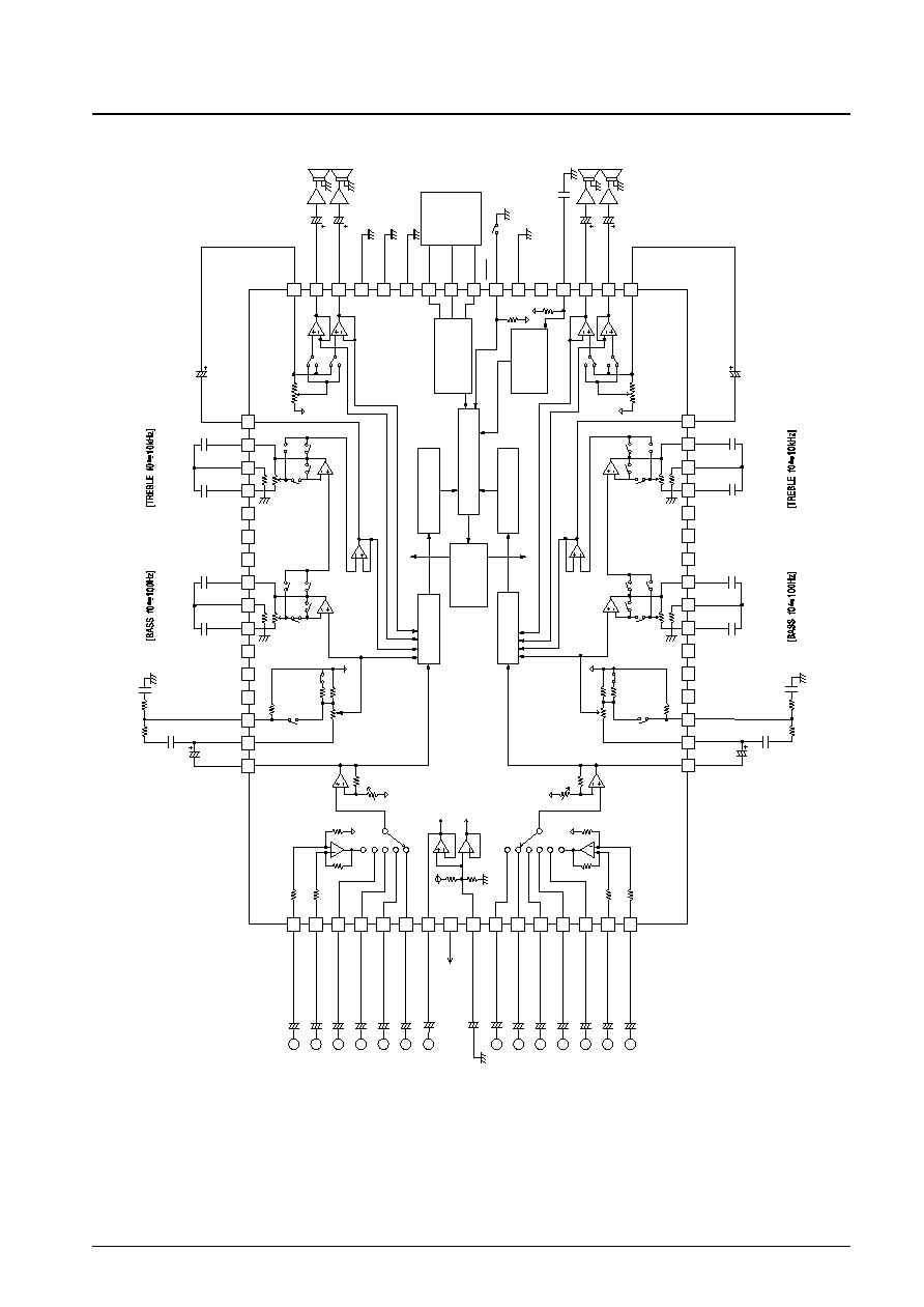
Overview
The LC75412E and 75412W are electronic volume
controllers that enable control of volume, balance, fader,
bass/treble, loudness, input switching, and input gain
using only a small number of external components.
Functions
∑ Volume: 0 dB to ≠79 dB in 1-dB steps, and ≠
(81
positions) Balance function with separate L/R
control
∑ Fader: rear output or front output can be attenuated
across 16 positions (in 1-dB steps from 0 dB to
≠2 dB, 2-dB steps from ≠2 dB to ≠20 dB, 10-dB
steps from ≠20 dB to ≠30 dB, and ≠45 dB,
≠60 dB, ≠
)
∑ Bass/treble: Each band can be controlled in 2-dB steps
from ±0 dB to ±18 dB.
∑ Input gain: 0 dB to +18.75 dB (1.25-dB steps)
amplification is possible for the input signal.
∑ Input switching: Six input signals can be selected for
Left and for Right (five are single-
ended inputs and one is a differential
input.)
∑ Loudness: A tap is output from the ≠32 dB position of a
volume control resistor ladder. A loudness
function can be implemented by connecting
an external RC circuit.
Features
∑ On-chip buffer amplifier cuts down number of external
components
∑ Low switching noise generated by on-chip switch
through use of silicon gate CMOS process, for low
switching noise when there is no signal
∑ Low switching noise when there is a signal due to use
of on-chip zero-cross switching circuit
∑ On-chip 1/2 VDD reference voltage circuit
∑ Controls performed with serial input (CCB)
LC75412E, 75412W
SANYO Electric Co.,Ltd. Semiconductor Company
TOKYO OFFICE Tokyo Bldg., 1-10, 1 Chome, Ueno, Taito-ku, TOKYO, 110-8534 JAPAN
Electronic Volume Controller
for Car Audio Systems
CMOS IC
Any and all SANYO products described or contained herein do not have specifications that can handle
applications that require extremely high levels of reliability, such as life-support systems, aircraft's
control systems, or other applications whose failure can be reasonably expected to result in serious
physical and/or material damage. Consult with your SANYO representative nearest you before using
any SANYO products described or contained herein in such applications.
SANYO assumes no responsibility for equipment failures that result from using products at values that
exceed, even momentarily, rated values (such as maximum ratings, operating condition ranges, or other
parameters) listed in products specifications of any and all SANYO products described or contained
herein.
∑ CCB is a trademark of SANYO ELECTRIC CO., LTD.
∑ CCB is SANYO's original bus format and all the bus
addresses are controlled by SANYO.
No. 7053-4/21
LC75412E, 75412W
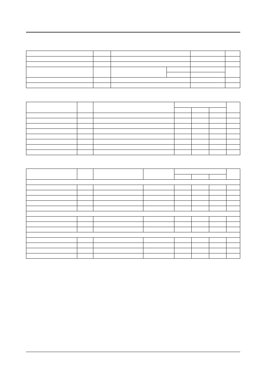
Parameter
Symbol
Conditions
Ratings
Unit
Maximum supply voltage
V
DD
max
V
DD
11
V
Maximum input voltage
V
IN
max
All input pins
V
SS
≠ 0.3 to V
DD
+ 0.3
V
Allowable power dissipation
Pd max
Ta
85∞C, when mounted on board
QIP64E
680
mW
SQFP64
800
Operating temperature
Topr
≠40 to +85
∞C
Storage temperature
Tstg
≠50 to +125
∞C
Specifications
Absolute Maximum Ratings
at Ta = 25∞C, V
SS
= 0 V
Parameter
Symbol
Conditions
Ratings
Unit
min
typ
max
Supply voltage
V
DD
V
DD
6.0
10
V
Input high-level voltage
V
IH
CL, DI, CE
4.0
10
V
Input low-level voltage
V
IL
CL, DI, CE
V
SS
1.0
V
Input amplitude voltage
V
IN
V
SS
V
DD
Vp-p
Input pulse width
T¯W
CL
1
µs
Setup time
Tsetup
CL, DI, CE
1
µs
Hold time
Thold
CL, DI, CE
1
µs
Operating frequency
fopg
CL
500
kHz
Allowable Operating Ranges
at Ta = 25∞C, V
SS
= 0 V
Parameter
Symbol
Pin Name
Conditions
Ratings
Unit
min
typ
max
[Input block]
Input resistance
Rin
L1 to L4, L6, R1 to R4, R6
25
50
100
k
Minimum input gain
Ginmin
L1 to L4, L6, R1 to R4, R6
≠1
0
+1
dB
Maximum input gain
Ginmax
+16.5
+18.75
+21
dB
Step setting error
ATerr
±0.5
dB
L/R balance
BAL
±0.5
dB
[Volume Block]
Input resistance
Rvr
LVRIN, RVRIN, loudness off
25
50
100
k
Step setting error
ATerr
±0.5
dB
L/R balance
BAL
±0.5
dB
[Tone block]
Step setting error
ATerr
±1.0
dB
Bass control range
Gbass
max. boost/cut
±15
±18
±21
dB
Treble control range
Gtre
max. boost/cut
±15
±18
±21
dB
L/R balance
BAL
±0.5
dB
Electrical Characteristics
at Ta = 25∞C, V
DD
= 9 V, V
SS
= 0 V
Continued on next page.
No. 7053-5/21
LC75412E, 75412W
Parameter
Symbol
Pin Name
Conditions
Ratings
Unit
min
typ
max
[Fader Block]
Input resistance
Rfed
LFIN, RFIN
25
50
100
k
0dB to ≠2dB
±0.5
dB
Step setting error
ATerr
≠2dB to ≠20dB
±1
dB
≠20dB to ≠30dB
±2
dB
≠30dB to ≠60dB
±3
dB
L/R balance
BAL
±0.5
dB
[General]
Total harmonic distortion
THD (1)
V
IN
= 0dBV, f = 1 kHz
0.004
0.01
%
THD (2)
V
IN
= ≠10dBV, f = 10 kHz
0.006
0.01
%
Input crosstalk
CT
V
IN
= 1Vrms, f = 1 kHz
80
88
dB
L/R crosstalk
CT
V
IN
= 1Vrms, f = 1 kHz
80
88
dB
Maximum attenuated output
Vomin (1) V
IN
= 1Vrms, f = 1 kHz
80
88
dB
Vomin (2)
V
IN
= 1Vrms, f = 1 kHz
90
95
dB
INMUTE, fader ≠
Output noise voltage
V
N
(1)
Flat overall, IHF-A filter
5
10
µV
V
N
(2)
Flat overall, 20 to 20 kHzBPF
7
15
µV
Current drain
I
DD
55
60
mA
Input high-level current
I
IH
CL, DI, CE, V
IN
= 9 V
10
µA
Input low-level current
I
IL
CL, DI, CE, V
IN
= 0 V
≠10
µA
Maximum input voltage
V
CL
THD = 1%, R
L
= 10 k
2.3
2.5
Vrms
flat overall, f
IN
= 1 kHz
Common-mode rejection ratio
CMRR
V
IN
= 0 dB, f = 1 kHz
70
dB
Continued from preceding page.
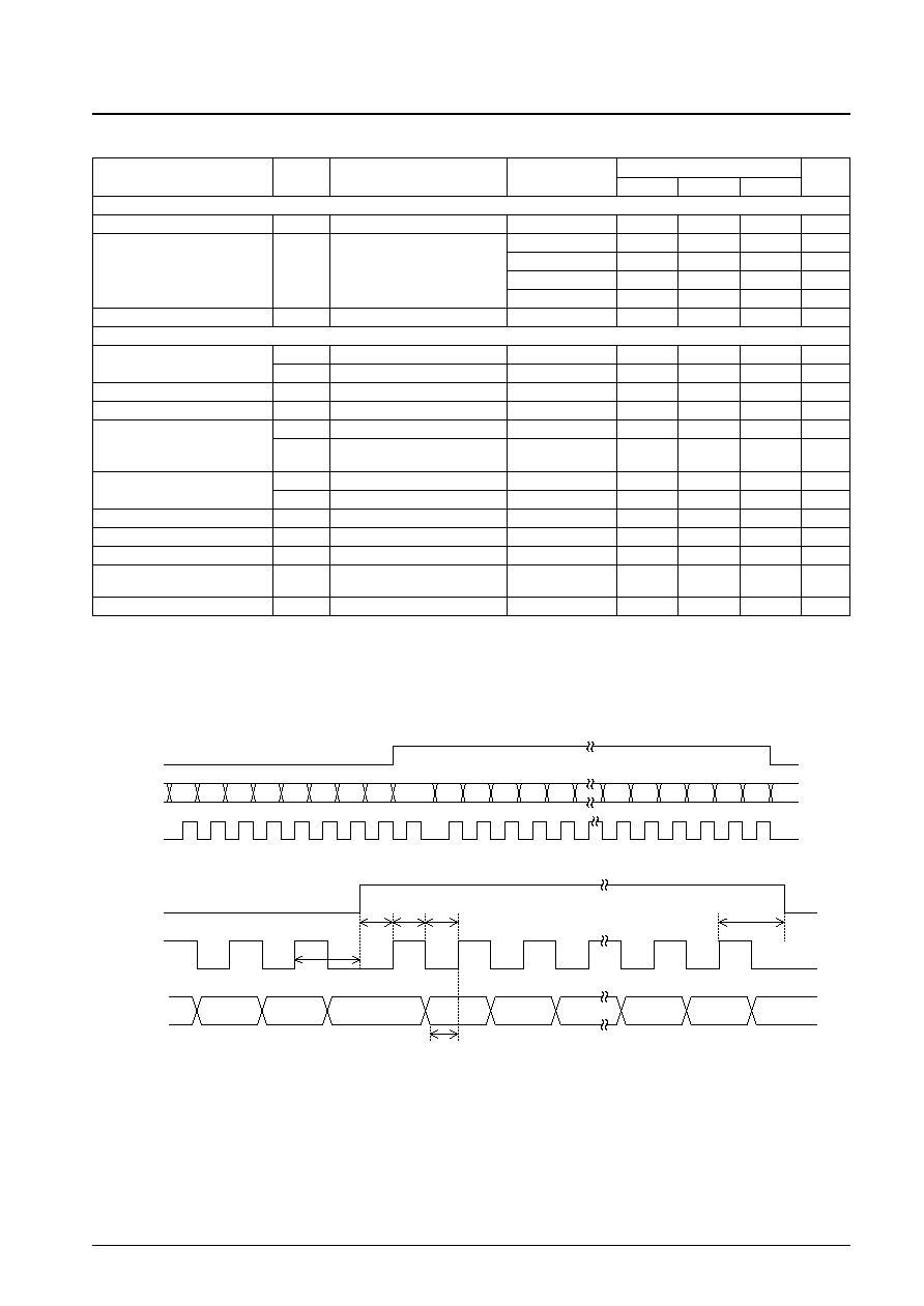
Control Timing and Data Format
To control the LC75412E and LC75412W input specified serial data to the CE, CL, and DI pins.
The data configuration consists of a total of 52 bits broken down into 8 address bits and 44 data bits.
CE
DI
D43
D42
D41
D40
D39
D38
D5
D4
D3
D2
D0 D1
A3
A2
A1
A0
B3
B2
B1
B0
CL
1
µ
s
min
1
µ
s
min
1
µ
s min
T
DEST
1
µ
s
min
1
µ
s
min
1
µ
s
min
CE
DI
CL