 | –≠–ª–µ–∫—Ç—Ä–æ–Ω–Ω—ã–π –∫–æ–º–ø–æ–Ω–µ–Ω—Ç: LC7573NM | –°–∫–∞—á–∞—Ç—å:  PDF PDF  ZIP ZIP |
LC7573N, 7573NM
1/2 Duty VFD Driver for Frequency Display
CMOS LSI
Ordering number : EN
*
3587B
SANYO Electric Co.,Ltd. Semiconductor Bussiness Headquarters
TOKYO OFFICE Tokyo Bldg., 1-10, 1 Chome, Ueno, Taito-ku, TOKYO, 110-8534 JAPAN
O2095HA (OT)/3242JN No.3587-1/10
Overview
The LC7573N and LC7573NM are 1/2 duty VFD drivers
that can be used for electronic tuning frequency display
and other applications under the control of a controller.
These products can directly drive VFDs with up to 38
segments.
Features
∑ 38 segment outputs
∑ Noise reduction circuits are built into the output drivers.
∑ Serial data input supports CCB* format
communications with the system controller.
∑ Switching between digital and analog dimmers under
serial data control
∑ High generality since display data is displayed without
the intervention of a decoder
∑ All segments can be turned off with the BLK pin
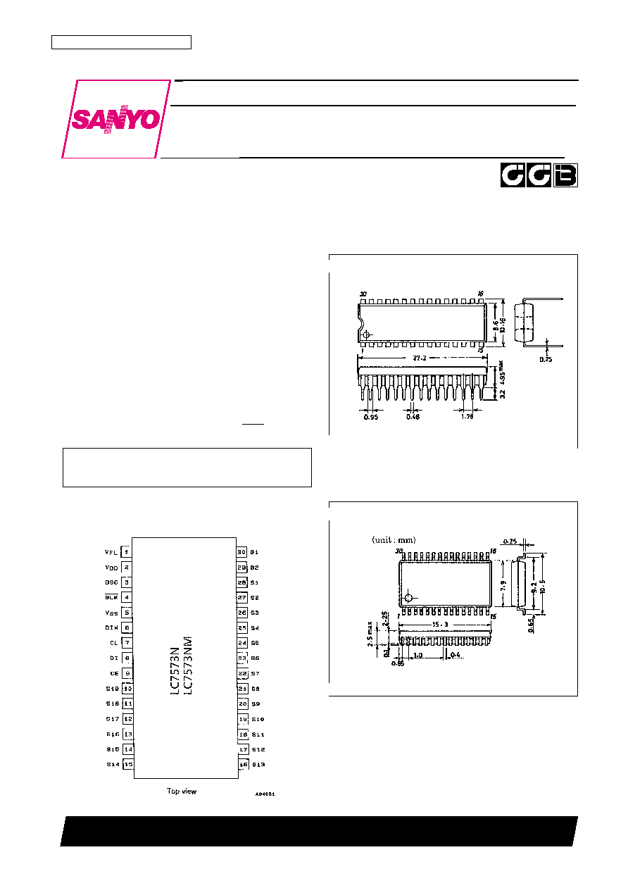
Pin Assignment
Package Dimensions
unit: mm
3061-DIP30S
Preliminary
SANYO: DIP30S
[LC7573N]
∑ CCB is a trademark of SANYO ELECTRIC CO., LTD.
∑ CCB is SANYO's original bus format and all the bus
addresses are controlled by SANYO.
unit: mm
3073A-MFP30S
SANYO: MFP30S
[LC7573NM]

Specifications
Absolute Maximum Ratings
at Ta = 25∞C, V
SS
= 0 V
Allowable Operating Ranges
at Ta = ≠40 to +85∞C, V
DD
= 4.5 to 5.5 V, V
SS
= 0 V
Electrical Characteristics
in the Allowable Operating Ranges
No. 3587-2/10
LC7573N, 7573NM
Parameter
Symbol
Conditions
Ratings
Unit
Maximum supply voltage
V
DD
max
V
DD
≠0.3 to +6.5
V
V
FL
max
V
FL
≠0.3 to +21.0
V
Input voltage
V
IN
1
DI, CL, CE, BLK, DIM
≠0.3 to +6.5
V
V
IN
2
OSC
≠0.3 to V
DD
+ 0.3
V
Output voltage
V
OUT
1
S1 to S19, G1, G2
≠0.3 to V
FL
+ 0.3
V
V
OUT
2
OSC
≠0.3 to V
DD
+ 0.3
V
Output current
I
OUT
1
S1 to S19
5
mA
I
OUT
2
G1, G2
30
mA
Allowable power dissipation
Pd max
Ta = 85∞C
150
mW
Operating temperature
Topr
≠40 to +85
∞C
Storage temperature
Tstg
≠50 to +125
∞C
Parameter
Symbol
Conditions
min
typ
max
Unit
Supply voltage
V
DD
V
DD
4.5
5.0
5.5
V
V
FL
V
FL
8
12
18
V
Input high level voltage
V
IH
DI, CL, CE, BLK
0.8 V
DD
5.5
V
Input low level voltage
V
IL
DI, CL, CE, BLK
0
0.2 V
DD
V
Guaranteed oscillator range
f
OSC
OSC
0.4
1.6
3.0
MHz
Recommended external
R
OSC
OSC
12
k
resistance
Recommended external
C
OSC
OSC
50
pF
capacitance
Low level clock pulse width
t
¯L
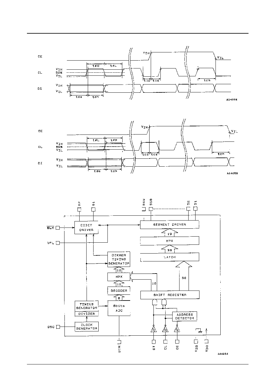
CL: Figure 1
0.5
µs
High level clock pulse width
t
¯H
CL: Figure 1
0.5
µs
Data setup time
t
ds
DI, CL: Figure 1
0.5
µs
Data hold time
t
dh
DI, CL: Figure 1
0.5
µs
CE wait time
t
cp
CE, CL: Figure 1
0.5
µs
CE setup time
t
cs
CE, CL: Figure 1
0.5
µs
CE hold time
t
ch
CE, CL: Figure 1
0.5
µs
BLK switching time
t
c
BLK, CE: Figure 3
10
µs
Input voltage range
V
IN
DIM
0
+5.5
V
Parameter
Symbol
Conditions
min
typ
max
Unit
Input high level current
I
IH
DI, CL, CE, BLK, DIM: V
I
= 5.5 V
5
µA
Input low level current
I
IL
DI, CL, CE, BLK, DIM: V
I
= 0 V
≠5
µA
V
OH
1
S1 to S19: I
O
= 2 mA
V
FL
≠ 0.6
V
Output high level voltage
V
OH
2
G1, G2: I
O
= 25 mA
V
FL
≠ 0.6
V
Output low level voltage
V
OL
S1 to S19, G1, G2: I
O
= ≠5 µA, Ta = 25∞C
0.125
0.25
0.5
V
Oscillator frequency
f
OSC
R
OSC
= 12 k
, C
OSC
= 50 pF
1.6
MHz
Hysteresis voltage
V
H
DI, CL, CE, BLK
0.5
V
A/D converter linearity error
Err
DIM
≠1/2
+1/2
LSB
Current drain
I
DD
Outputs open: f
OSC
= 1.6 MHz
5
mA
1. When CL is stopped at the low level
2. When CL is stopped at the high level
Figure 1
Block Diagram
No. 3587-3/10
LC7573N, 7573NM
Pin Functions
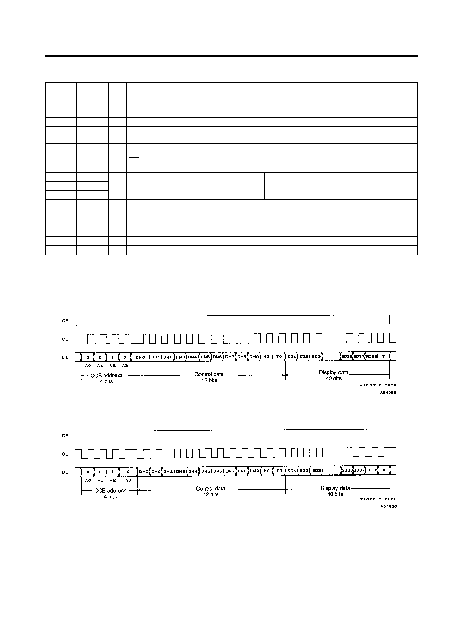
Serial Data Transfer Format
1. When CL is stopped at the low level
2. When CL is stopped at the high level
Figure 2
No. 3587-4/10
LC7573N, 7573NM
Pin No.
Pin
I/O
Function
Handling
when unused
1
V
FL
--
Driver block power supply. A voltage of between 8.0 and 18.0 V must be supplied.
--
2
V
DD
--
Logic block power supply. A voltage of between 4.5 and 5.5 V must be supplied.
--
5
V
SS
--
Ground. Must be connected to the system ground.
--
3
OSC
I/O
Oscillator connection. An oscillator circuit is formed by connecting an external resistor and capacitor
to this pin.
V
DD
Display off control input
4
BLK
I
BLK = low (V
SS
): Display off (G1 and G2 = low)
GND
BLK = high (V
DD
): Display on
Note that serial data can be transferred while the display is turned off.
7
CL
Serial data transfer inputs. These pins must be
CL: synchronization clock
8
DI
I
connected to the system controller.
DI: transfer data
GND
9
CE
CE: chip enable
When the analog dimmer is selected, the analog voltage applied to this pin controls the duty of the G1
and G2 digit output pins. Since a 6-bit A/D converter is applied to this analog voltage and that result is
6
DIM
I
input to a decoder that provides a built-in dimmer curve, the relationship between the analog voltage
GND
and the duty can be specified as a mask program. Note that 63/96 ∑ V
DD
is the full-scale level for the
6-bit A/D converter.
30, 29
G1, G2
O
Digit outputs. The frame frequency f
O
is (f
OSC
/4096) Hz
Open
28 to 10
S1 to S19
O
Segment outputs for displaying the display data transferred by serial data input.
Open
CCB address: Transfer 0010
B
, as shown in Figure 2.
M0:
Digital/analog dimmer selection data
M0 = 0 ....................................Digital dimmer
M0 = 1 ....................................Analog dimmer
DM0 to DM9: Dimmer data
This data controls the duty of the G1 and G2 digit output pins when the digital dimmer is selected.
This data consists of 10 bits, of which DM0 is the LSB. Note that display intensity can be adjusted by
controlling the duty of the G1 and G2 digit output pins. (The DM0 to DM9 dimmer data is ignored
when the analog dimmer is selected.)
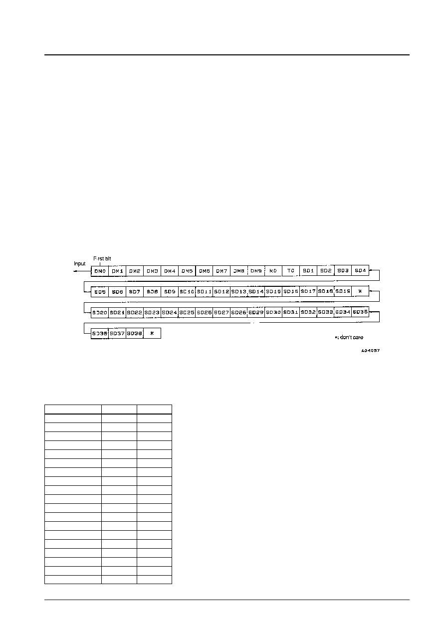
SD1 to SD38: Display data
SD1 to SD19...........................Display data for the G1 digit output pin
SD20 to SD38.........................Display data for the G2 digit output pin
SDn (n = 1 to 38) = 1..............Display on
SDn (n = 1 to 38) = 0..............Display off
T0:
Test data
The T0 bit must be set to 0.
Serial Data Format
Correspondence between Display Data (SD1 to SD38) and Segment Output Pins
No. 3587-5/10
LC7573N, 7573NM
Segment output pin
G1
G2
S1
SD1
SD20
S2
SD2
SD21
S3
SD3
SD22
S4
SD4
SD23
S5
SD5
SD24
S6
SD6
SD25
S7
SD7
SD26
S8
SD8
SD27
S9
SD9
SD28
S10
SD10
SD29
S11
SD11
SD30
S12
SD12
SD31
S13
SD13
SD32
S14
SD14
SD33
S15
SD15
SD34
S16
SD16
SD35
S17
SD17
SD36
S18
SD18
SD37
S19
SD19
SD38