 | –≠–ª–µ–∫—Ç—Ä–æ–Ω–Ω—ã–π –∫–æ–º–ø–æ–Ω–µ–Ω—Ç: LC75742W | –°–∫–∞—á–∞—Ç—å:  PDF PDF  ZIP ZIP |
Ordering number : EN6142
43099TH (OT) No. 6142-1/18
Overview
The LC75742E and LC75742W are 1/2 duty VFD drivers
that can be used for electronic tuning frequency display
and other applications under the control of a micro-
controller. These products can directly drive VFDs with
up to 82 segments. It also includes a key scan circuit and
can support input from up to 30 keys and can thus reduce
the number of lines to the front panel in application
systems.
Features
∑ Key input from up to 30 keys
(Key scans are only performed when keys are pressed.)
∑ 82 segment outputs.
∑ Noise reduction circuits are built into the output drivers.
∑ Serial data I/O supports CCB format communication
with the system controller.
∑ Dimmer and sleep mode can be controlled by serial data
input.
∑ High generality since display data is displayed without
the intervention of a decoder.
∑ All segments can be turned off with the BLK pin.
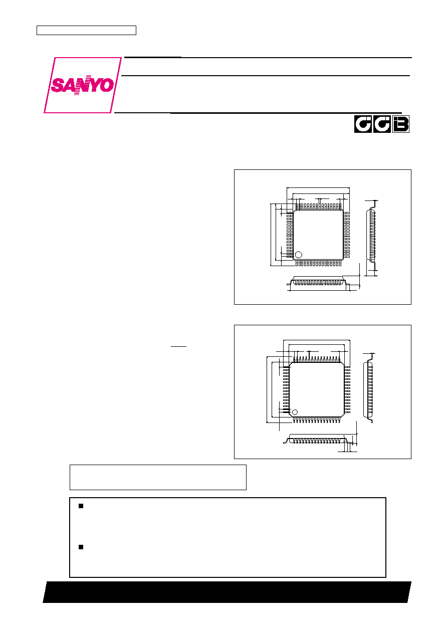
Package Dimensions
unit: mm
3151-QFP64E
unit: mm
3190-SQFP64
14.0
17.2
1.0
1.0
1.6
0.15
0.35
0.1
15.6
0.8
0.8
3.0max
1
16
17
32
33
48
49
64
2.7
14.0
17.2
1.0
1.0
1.6
0.8
SANYO: QFP64E (QIP64E)
[LC75742E]
LC75742E, 75742W
SANYO Electric Co.,Ltd. Semiconductor Company
TOKYO OFFICE Tokyo Bldg., 1-10, 1 Chome, Ueno, Taito-ku, TOKYO, 110-8534 JAPAN
1/2 Duty VFD Driver with Key Input Function
CMOS IC
Any and all SANYO products described or contained herein do not have specifications that can handle
applications that require extremely high levels of reliability, such as life-support systems, aircraft's
control systems, or other applications whose failure can be reasonably expected to result in serious
physical and/or material damage. Consult with your SANYO representative nearest you before using
any SANYO products described or contained herein in such applications.
SANYO assumes no responsibility for equipment failures that result from using products at values that
exceed, even momentarily, rated values (such as maximum ratings, operating condition ranges, or other
parameters) listed in products specifications of any and all SANYO products described or contained
herein.
∑ CCB is a trademark of SANYO ELECTRIC CO., LTD.
∑ CCB is SANYO's original bus format and all the bus
addresses are controlled by SANYO.
10.0
12.0
1.25
0.5
1.25
1.25
0.5
1.25
0.18
12.0
1
16
17
32
33
48
49
64
10.0
0.5
1.7max
0.5
0.1
0.15
SANYO: SQFP64
[LC75742W]
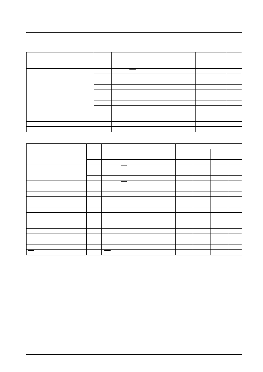
Specifications
Absolute Maximum Ratings
at Ta = 25∞C, V
SS
= 0 V
Allowable Operating Ranges
at Ta = ≠40 to +85∞C, V
DD
= 4.5 to 5.5 V, V
SS
= 0 V
Note: Since DO is an open-drain output, these values will vary with the pull-up resistance R
PU
and the load capacitance C
L
.
No. 6142-2/18
LC75742E, LC75742W
Parameter
Symbol
Conditions
Ratings
Unit
min
typ
max
Supply voltage
V
DD
V
DD
4.5
5.0
5.5
V
V
FL
V
FL
8
12
18
V
V
IH
1
DI, CL, CE, BLK
0.8 V
DD
5.5
V
High-level input voltage
V
IH
2
OSCI
0.8 V
DD
V
DD
V
V
IH
3
KI1 to KI5
0.6 V
DD
V
DD
V
Low-level input voltage
V
IL
DI, CL, CE, BLK, OSCI, KI1 to KI5
0
0.2 V
DD
V
Guaranteed oscillator frequency range
f
OSC
OSCI, OSCO
0.4
1.6
3.0
MHz
Recommended external resistor value
R
OSC
OSCI, OSCO
4.7
20
100
k
Recommended external capacitor value
C
OSC
OSCI, OSCO
22
47
100
pF
Clock low-level pulse width
t
¯L
CL : See figure 1.
160
ns
Clock high-level pulse width
t
¯H
CL : See figure 1.
160
ns
Data setup time
t
ds
DI, CL : See figure 1.
160
ns
Data hold time
t
dh
DI, CL : See figure 1.
160
ns
CE wait time
t
cp
CE, CL : See figure 1.
160
ns
CE setup time
t
cs
CE, CL : See figure 1.
160
ns
CE hold time
t
ch
CE, CL : See figure 1.
160
ns
DO output delay time
t
dc
DO: R
PU
= 4.7 k
, C
L
= 10 pF
*
: See figure 1.
1.5
µs
DO rise time
t
dr
DO: R
PU
= 4.7 k
, C
L
= 10 pF
*
: See figure 1.
1.5
µs
BLK switching time
t
c
BLK, CE : See figure 4.
10
µs
Parameter
Symbol
Conditions
Ratings
Unit
Maximum Supply voltage
V
DD
max
V
DD
≠0.3 to +6.5
V
V
FL
max
V
FL
≠0.3 to +21.0
V
Input voltage
V
IN
1
DI, CL, CE, BLK
≠0.3 to +6.5
V
V
IN
2
OSCI, KI1 to KI5
≠0.3 to V
DD
+0.3
V
V
OUT
1
S1 to S41, G1, G2
≠0.3 to V
FL
+0.3
V
Output voltage
V
OUT
2
OSCO, KS1 to KS6
≠0.3 to V
DD
+0.3
V
V
OUT
3
DO
≠0.3 to +6.5
V
I
OUT
1
S1 to S41
6
mA
Output current
I
OUT
2
G1, G2
60
mA
I
OUT
3
KS1 to KS6
1
mA
Allowable power dissipation
Pd max
Ta = 85∞C (LC75742E)
400
mW
Ta = 85∞C (LC75742W)
300
mW
Operating temperature
Topr
≠40 to +85
∞C
Storage temperature
Tstg
≠50 to +150
∞C
∑ When stopped with CL at the low level
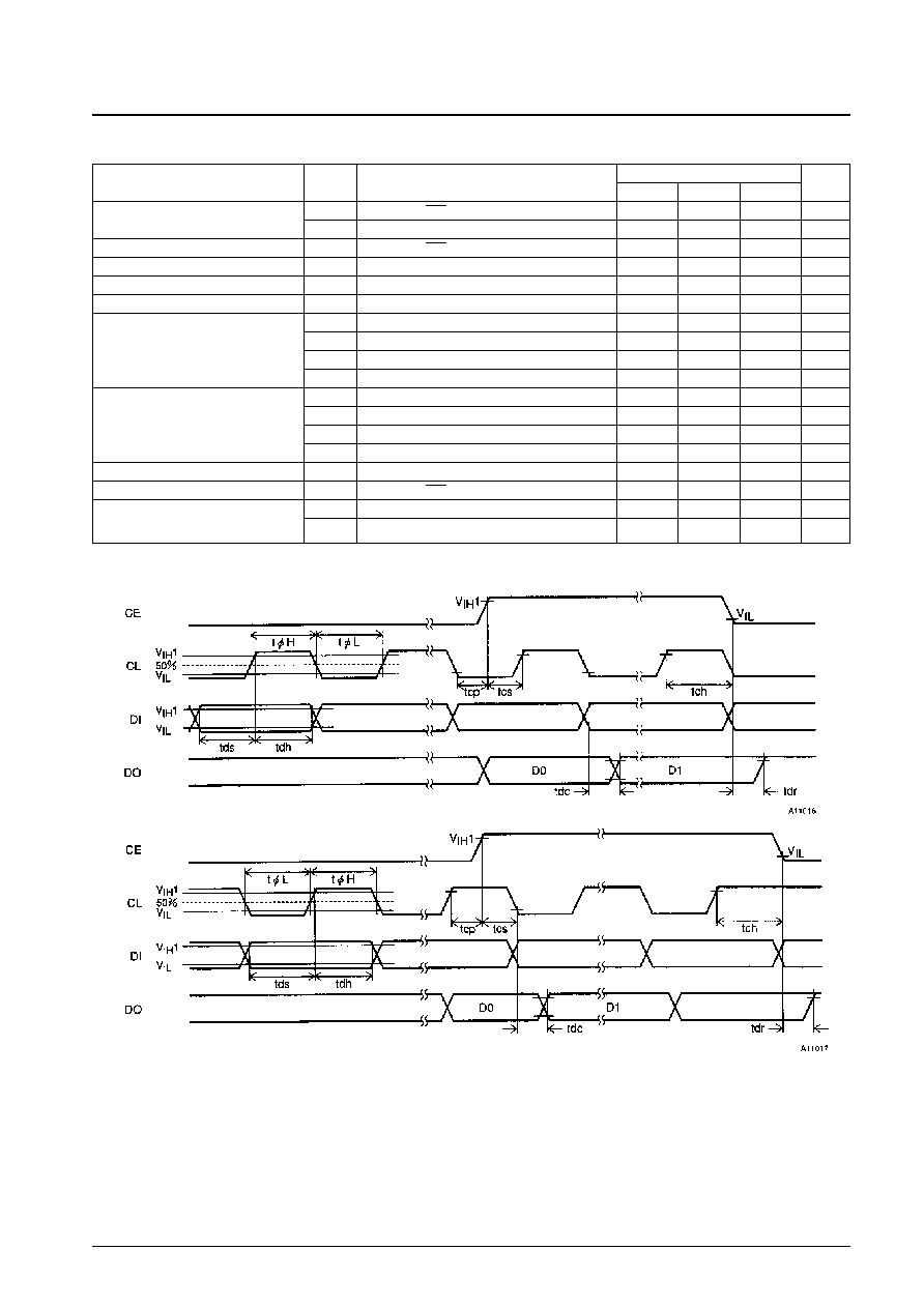
No. 6142-3/18
LC75742E, LC75742W
∑ When stopped with CL at the high level
Figure 1
Parameter
Symbol
Conditions
Ratings
Unit
min
typ
max
High-level input current
I
IH
1
DI, CL, CE, BLK: V
IN
= 5.5 V
5
µA
I
IH
2
OSCI: V
IN
= V
DD
5
µA
Low-level input current
I
IL
DI, CL, CE, BLK, OSCI: V
IN
= 0 V
≠5
µA
Input floating voltage
V
IF
KI1 to KI5
0.05 V
DD
V
Pull-down resistance
R
PD
KI1 to KI5: V
DD
= 5.0 V
50
100
250
k
Output off leakage current
I
OFFH
DO: V
O
= 5.5 V
5
µA
V
OH
1
S1 to S41: I
O
= ≠2 mA
V
FL
≠ 0.6
V
High-level output voltage
V
OH
2
G1, G2: I
O
= ≠50 mA
V
FL
≠ 1.3
V
V
OH
3
OSCO: I
O
= ≠0.5 mA
V
DD
≠ 2.0
V
V
OH
4
KS1 to KS6: I
O
= ≠500 µA
V
DD
≠ 1.2
V
DD
≠ 0.5
V
DD
≠ 0.2
V
V
OL
1
S1 to S41, G1, G2: I
O
= 50 µA
0.5
V
Low-level output voltage
V
OL
2
OSCO: I
O
= 0.5 mA
2.0
V
V
OL
3
KS1 to KS6: I
O
= 25 µA
0.2
0.5
1.5
V
V
OL
4
DO: I
O
= 1 mA
0.1
0.5
V
Oscillator frequency
f
OSC
R
OSC
= 20 k
, C
OSC
= 47 pF
1.6
MHz
Hysteresis voltage
V
H
DI, CL, CE, BLK, KI1 to KI5
0.1 V
DD
V
Current drain
I
DD
1
Sleep mode
5
µA
I
DD
2
Outputs open: f
OSC
= 1.6 MHz
10
mA
Electrical Characteristics
in the Allowable Operating Ranges
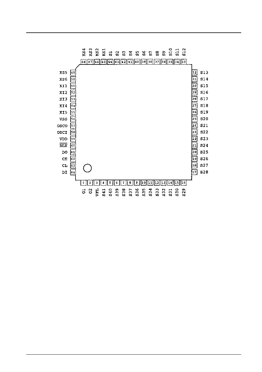
Pin Assignment
No. 6142-4/18
LC75742E, LC75742W
Top view
LC75742E
LC75742W
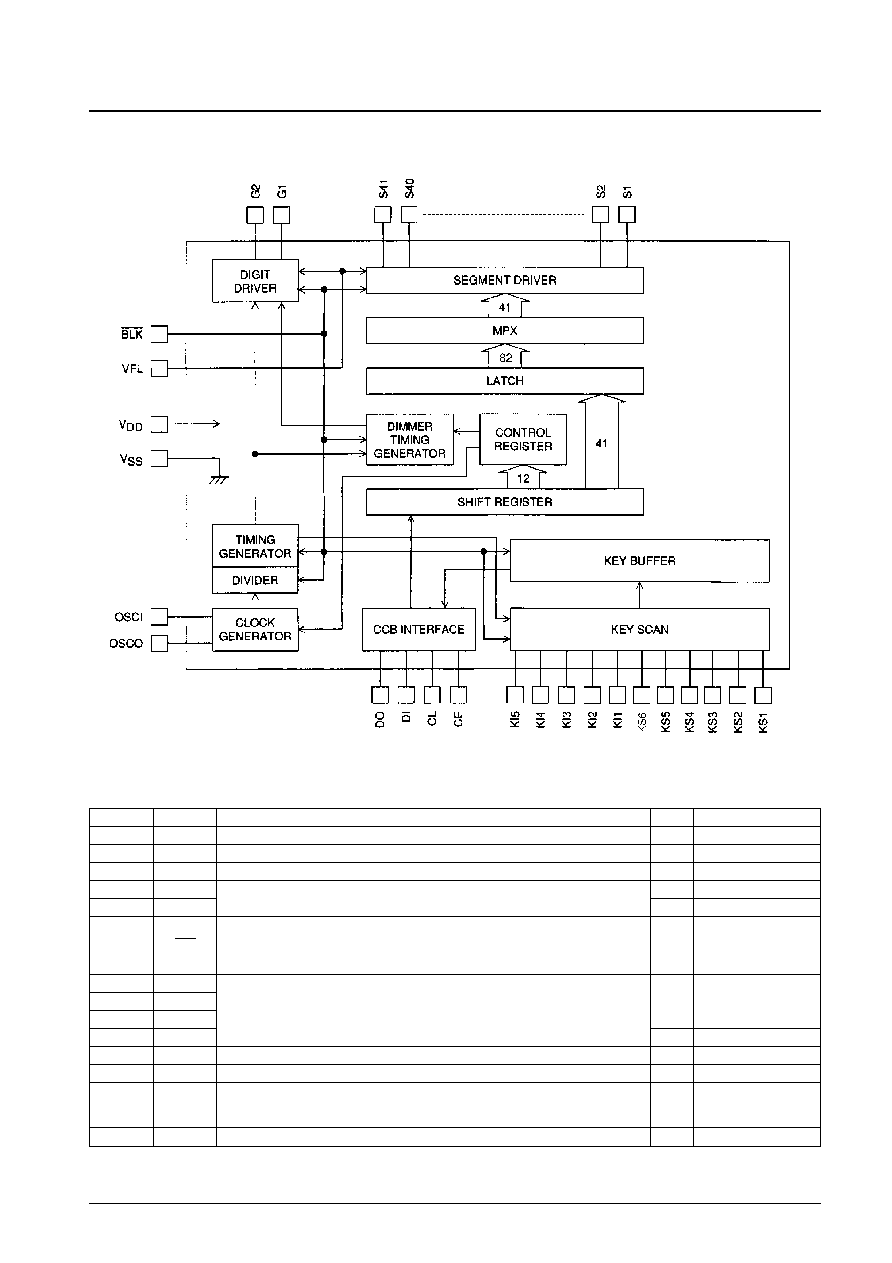
Block Diagram
Pin Descriptions
No. 6142-5/18
LC75742E, LC75742W
Pin No.
Pin
Function
I/O
Handling when unused
3
V
FL
Driver block power supply. Applications must provide a voltage in the range 8.0 to 18.0 V.
--
--
59
V
DD
Logic block power supply. Applications must provide a voltage in the range 4.5 to 5.5 V.
--
--
56
V
SS
Power supply ground. This pin must be connected to the system ground.
--
--
58
OSCI
I
GND
57
OSCO
O
OPEN
Reset signal input used to initialize the IC internal state. During a reset,
60
BLK
the display is turned off forcibly regardless of the internal display data.
I
GND
Also note that the internal key data is all reset to 0 and key scan operations are disabled.
However, serial data input is possible in this state.
63
CL
64
DI
I
GND
62
CE
61
DO
O
OPEN
1, 2
G1, G2
Digit outputs. The frame frequency f
O
is (f
OSC
/4096) Hz.
O
OPEN
44 to 4
S1 to S41
Segment outputs that display the display data transferred over the serial interface.
O
OPEN
Key scan outputs. Normally, when a key matrix is formed, diodes are inserted in the key
45 to 50
KS1 to KS6
scan timing lines to prevent shorts. However, since this IC uses unbalanced CMOS outputs
O
OPEN
in the output transistor circuit, the IC will not be damaged if these outputs are shorted.
51 to 55
KI1 to KI5
Key scan inputs. Pull-down resistors are built into the IC internal pin circuits.
I
GND
Serial data interface. These pins must be connected to the system microcontroller.
Note that since DO is an open-drain output, a pull-up resistor is required.
CL: Synchronization clock
DI: Transfer data
CE: Chip enable
DO: Output data
Oscillator circuit connections. An oscillator circuit is formed by connecting a resistor and a
capacitor externally to these pins.