Ordering number : EN5964
101698RM (OT) No. 5964-1/13
LC75750E, 75750W
SANYO Electric Co.,Ltd. Semiconductor Bussiness Headquarters
TOKYO OFFICE Tokyo Bldg., 1-10, 1 Chome, Ueno, Taito-ku, TOKYO, 110-8534 JAPAN
1/3 Duty VFD Driver
CMOS IC
Any and all SANYO products described or contained herein do not have specifications that can handle
applications that require extremely high levels of reliability, such as life-support systems, aircraft's
control systems, or other applications whose failure can be reasonably expected to result in serious
physical and/or material damage. Consult with your SANYO representative nearest you before using
any SANYO products described or contained herein in such applications.
SANYO assumes no responsibility for equipment failures that result from using products at values that
exceed, even momentarily, rated values (such as maximum ratings, operating condition ranges, or other
parameters) listed in products specifications of any and all SANYO products described or contained
herein.
Overview
The LC75750E and LC75750W are 1/3 duty VFD drivers
that can be used for electronic tuning frequency display
and other applications under the control of a micro-
controller. These products can directly drive VFDs with
up to 264 segments.
Features
∑ 264 segment outputs.
∑ Noise reduction circuits are built into the output drivers.
∑ Serial data input supports CCB format communication
with the system controller.
∑ Dimmer can be controlled by serial data input.
∑ High generality since display data is displayed without
the intervention of a decoder.
∑ All segments can be turned off with the BLK pin.
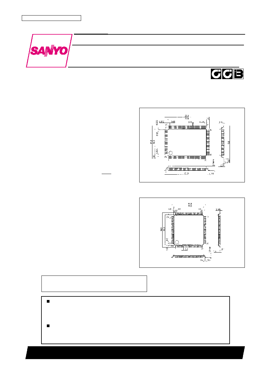
Package Dimensions
unit: mm
3151-QFP100E
unit: mm
3181B-SQFP100
SANYO: QFP100E (QIP100E)
[LC75750E]
SANYO: SQFP100
[LC75750W]
∑ CCB is a trademark of SANYO ELECTRIC CO., LTD.
∑ CCB is SANYO's original bus format and all the bus
addresses are controlled by SANYO.
No. 5964-2/13
LC75750E, 75750W
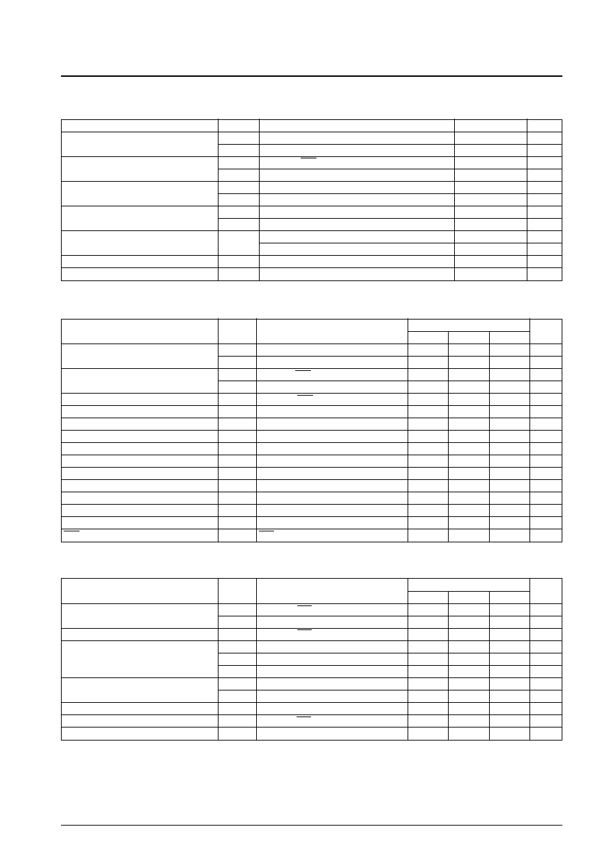
Parameter
Symbol
Conditions
Ratings
Unit
Maximum supply voltage
V
DD
max
V
DD
≠0.3 to +6.5
V
V
FL
max
V
FL
≠0.3 to +21.0
V
Input voltage
V
IN
1
DI, CL, CE, BLK
≠0.3 to +6.5
V
V
IN
2
OSCI
≠0.3 to V
DD
+0.3
V
Output voltage
V
OUT
1
S1 to S88, G1 to G3
≠0.3 to V
FL
+0.3
V
V
OUT
2
OSCO
≠0.3 to V
DD
+0.3
V
Output current
I
OUT
1
S1 to S88
6
mA
I
OUT
2
G1 to G3
60
mA
Allowable power dissipation
Pd max
Ta = 85∞C (LC75750E)
500
nW
Ta = 85∞C (LC75750W)
450
mW
Operating temperature
Topr
≠40 to +85
∞C
Storage temperature
Tstg
≠50 to +150
∞C
Specifications
Absolute Maximum Ratings
at Ta = 25∞C, V
SS
= 0V
Allowable Operating Ranges
at Ta = ≠40 to +85∞C, V
DD
= 4.5 to 5.5V, V
SS
= 0V
Parameter
Symbol
Conditions
Ratings
Unit
min
typ
max
Supply voltage
V
DD
V
DD
4.5
5.0
5.5
V
V
FL
V
FL
8
12
18
V
Input high-level voltage
V
IH
1
DI, Cl, CE, BLK
0.8 V
DD
5.5
V
V
IH
2
OSCI
0.8 V
DD
V
DD
V
Input low-level voltage
V
IL
DI, CL, CE, BLK, OSCI
0
0.2 V
DD
V
Guaranteed oscillator range
f
OSC
OSCI, OSCO
0.9
2.4
3.7
MHz
Recommended external resistance
R
OSC
OSCI, OSCO
2.2
12
47
K
Recommended external capacitance
C
OSC
OSCI, OSCO
15
33
100
pF
Low level clock pulse width
t
¯L
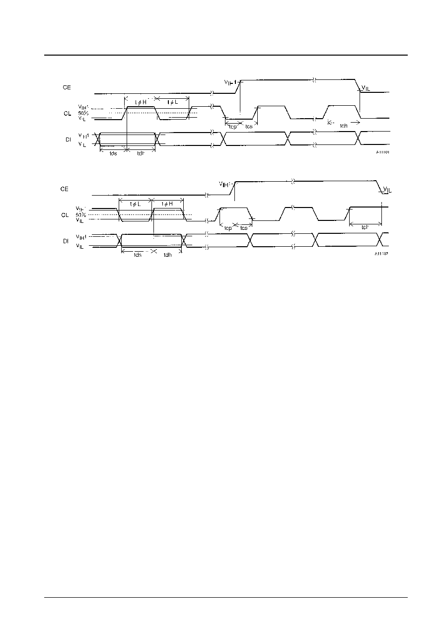
CL : Figure 1
160
ns
High level clock pulse width
t
¯H
CL : Figure 1
160
ns
Data setup time
t
ds
DI, CL : Figure 1
160
ns
Data hold time
t
dh
DI, CL : Figure 1
160
ns
CE wait time
t
cp
CE, CL : Figure 1
160
ns
CE setup time
t
cs
CE, CL : Figure 1
160
ns
CE hold time
t
ch
CE, CL : Figure 1
160
ns
BLK switching time
t
c
BLK, CE : Figure 3
10
µs
Electrical Characteristics
in the Allowable Operating Ranges
Parameter
Symbol
Conditions
Ratings
Unit
min
typ
max
Input high-level current
I
IH
1
DI, CL, CE, BLK : V
IN
= 5.5V
5
µA
I
IH
2
OSCI : V
IN
= V
DD
5
µA
Input low-level current
I
IL
DI, CL, CE, BLK, OSCI : V
IN
= 0V
≠5
µA
V
OH
1
S1 to S88 : I
O
= ≠2 mA
V
FL
≠ 0.6
V
Output high-level voltage
V
OH
2
G1 to G3 : I
O
= ≠50 mA
V
FL
≠ 1.3
V
V
OH
3
OSCO : I
O
= ≠0.5 mA
V
DD
≠ 2.0
V
Output low-level voltage
V
OL
1
S1 to S88, G1 to G3 : I
O
= 50 µA
0.5
V
V
OL
2
OSCO :I
O
= 0.5mA
2.0
V
Oscillator frequency
f
OSC
R
OSC
= 12 k
, C
OSC
= 33 pF
2.4
MHz
Hysteresis voltage
V
H
DI, CL, CE, BLK
0.1 V
DD
V
Current drain
I
DD
Outputs open : f
OSC
= 2.4 MHz
10
mA
No. 5964-5/13
LC75750E, 75750W
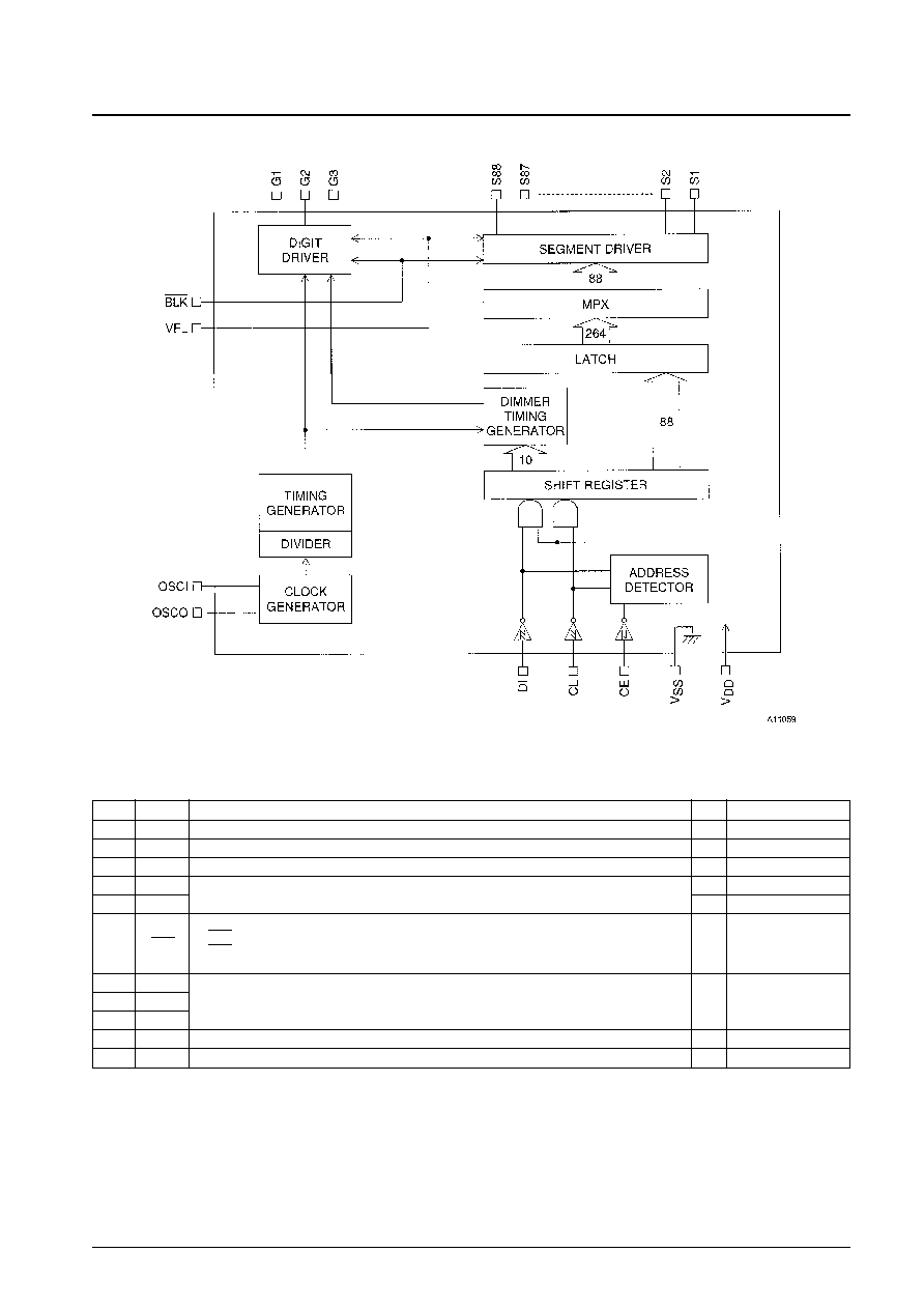
Block Diagram
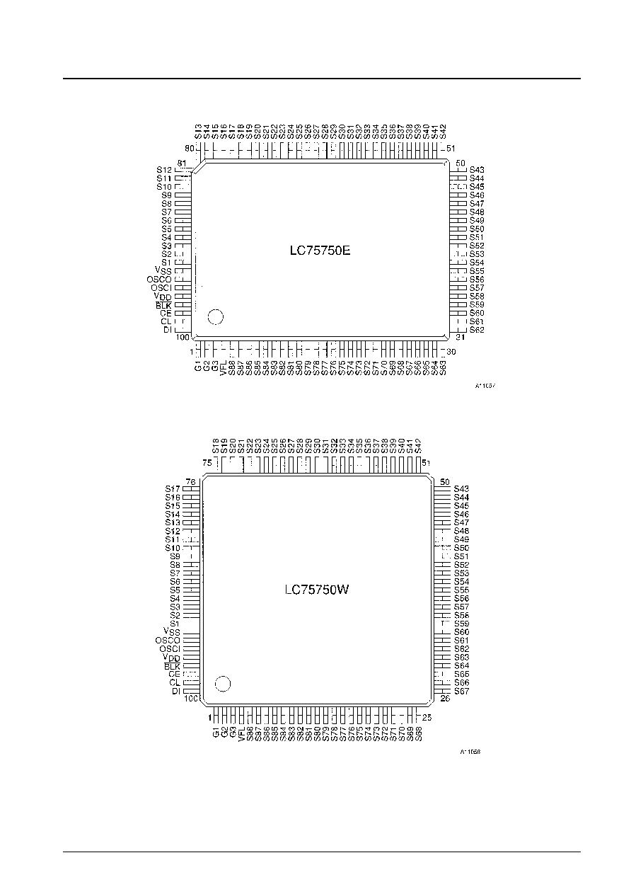
Pin Functions
Pin No.
Pin
Function
I/O
Handling when unused
4
V
FL
Driver block power supply. A voltage of between 8.0 and 18.0 V must be supplied.
--
--
96
V
DD
Logic block power supply. A voltage of between 4.5 and 5.5 V must be supplied.
--
--
93
V
SS
Power supply. Must be connected to the system ground.
--
--
95
OSCI
Oscillator connection. An oscillator circuit is formed by connecting an external resistor and
I
GND
94
OSCO
capacitor to these pins.
O
OPEN
Display off control input.
97
BLK
BLK = L (V
SS
) ...........Display off (S1 to S24, G1 to G3 = L)
I
GND
BLK = H (V
DD
) ..........Display on
Note that serial data can be transferred while the display is turned off.
99
CL
Serial data transfer inputs. These pins must be connected to the system microcontroller.
100
DI
CL : Synchronization clock DI : Transfer data CE : Chip enable
I
GND
98
CE
1 to 3
G1 to G3
Digit outputs. The frame frequency fo is (f
OSC
/6144)Hz.
O
OPEN
92 to 5 S1 to S88 Segment outputs for displaying the display data transferred by serial data input
O
OPEN