Ordering number : EN5915A
N1098RM (OT) No. 5915-1/27
LC75811E, 75811W
SANYO Electric Co.,Ltd. Semiconductor Bussiness Headquarters
TOKYO OFFICE Tokyo Bldg., 1-10, 1 Chome, Ueno, Taito-ku, TOKYO, 110-8534 JAPAN
1/8 to 1/10 Duty Dot Matrix LCD Display Controller/Driver
CMOS IC
Any and all SANYO products described or contained herein do not have specifications that can handle
applications that require extremely high levels of reliability, such as life-support systems, aircraft's
control systems, or other applications whose failure can be reasonably expected to result in serious
physical and/or material damage. Consult with your SANYO representative nearest you before using
any SANYO products described or contained herein in such applications.
SANYO assumes no responsibility for equipment failures that result from using products at values that
exceed, even momentarily, rated values (such as maximum ratings, operating condition ranges, or other
parameters) listed in products specifications of any and all SANYO products described or contained
herein.
∑ CCB is a trademark of SANYO ELECTRIC CO., LTD.
∑ CCB is SANYO's original bus format and all the bus
addresses are controlled by SANYO.
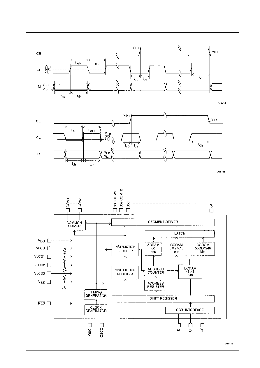
Overview
The LC75811E and LC75811W are 1/8 to 1/10 duty dot
matrix LCD display controller/drivers that supports the
display of characters, numbers, and symbols. In addition to
generating dot matrix LCD drive signals based on data
transferred serially from a microcontroller, the LC75811E
and LC75811W also provide on-chip character display ROM
and RAM to allow display systems to be implemented easily.
Features
∑ Controls and drives a 5
◊
7, 5
◊
8, or 5
◊
9 dot matrix LCD.
∑ Supports accessory display segment drive (up to 60
segments)
∑ Display technique: 1/8 duty 1/4 bias drive (5
◊
7 dots)
1/9 duty 1/4 bias drive (5
◊
8 dots)
1/10 duty 1/4 bias drive (5
◊
9 dots)
∑ Display digits: 12 digits
◊
1 line (5
◊
7 dots),
11 digits
◊
1 line (5
◊
8 or 5
◊
9 dots)
∑ Display control memory
CGROM: 240 characters (5
◊
7, 5
◊
8, or 5
◊
9 dots)
CGRAM: 16 characters (5
◊
7, 5
◊
8, or 5
◊
9 dots)
ADRAM: 12
◊
5 bits
DCRAM: 48
◊
8 bits
∑ Instruction function
Display on/off control
Display shift function
∑ Provides a backup function based on low power modes.
∑ Serial data input supports CCB format communication
with the system controller.
∑ Independent LCD drive block power supply VLCD
∑ Provides a RES pin for LSI internal initialization
∑ RC oscillator circuit
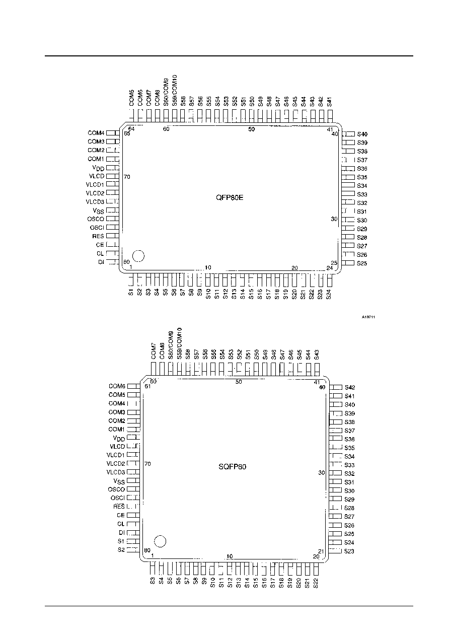
Package Dimensions
unit: mm
3174-QFP80E
unit: mm
3220-SQFP80
SANYO: QFP80E
[LC75811E]
SANYO: SQFP80
[LC75811W]
No. 5915-3/27
LC75811E, 75811W
Parameter
Symbol
Conditions
Ratings
Unit
Maximum supply voltage
V
DD
max
V
DD
≠0.3 to +7.0
V
V
LCD
max
V
LCD
≠0.3 to +11.0
V
V
IN
1
CE, CL, DI, RES
≠0.3 to +7.0
V
Input voltage
V
IN
2
OSCI
≠0.3 to V
DD
+ 0.3
V
V
IN
3
V
LCD
1, V
LCD
2, V
LCD
3
≠0.3 to V
LCD
+ 0.3
V
Output voltage
V
OUT
1
OSCO
≠0.3 to V
DD
+ 0.3
V
V
OUT
2
S1 to S60, COM1 to COM10
≠0.3 to V
LCD
+ 0.3
V
Output current
I
OUT
1
S1 to S60
300
µA
I
OUT
2
COM1 to COM10
3
mA
Allowable power dissipation
Pd max
Ta = 85∞C
200
mW
Operating temperature
Topr
≠40 to +85
∞C
Storage temperature
Tstg
≠55 to +125
∞C
Specifications
Absolute Maximum Ratings
at Ta = 25∞C, V
SS
= 0 V
Parameter
Symbol
Conditions
Ratings
Unit
min
typ
max
Supply voltage
V
DD
V
DD
2.7
6.0
V
V
LCD
V
LCD
4.5
10.0
V
V
LCD
1
V
LCD
1
3/4 V
LCD
V
LCD
V
Input voltage
V
LCD
2
V
LCD
2
2/4 V
LCD
V
LCD
V
V
LCD
3
V
LCD
3
1/4 V
LCD
V
LCD
V
Input high level voltage
V
IH
1
CE, CL, DI, RES
0.8 V
DD
6.0
V
V
IH
2
OSCI
0.7 V
DD
V
DD
V
Input low level voltage
V
IL
1
CE, CL, DI, RES
0
0.2 V
DD
V
V
IL
2
OSCI
0
0.3 V
DD
V
Recommended external resistance
R
OSC
OSCI, OSCO
33
k
Recommended external capacitance
C
OSC
OSCI, OSCO
220
pF
Guaranteed oscillation range
f
OSC
OSC
150
300
600
kHz
Data setup time
t
ds
CL, DI: Figure 2
160
ns
Data hold time
t
dh
CL, DI: Figure 2
160
ns
CE wait time
t
cp
CE, CL: Figure 2
160
ns
CE setup time
t
cs
CE, CL: Figure 2
160
ns
CE hold time
t
ch
CE, CL: Figure 2
160
ns
High level clock pulse width
t¯H
CL: Figure 2
160
ns
Low level clock pulse width
t¯L
CL: Figure 2
160
ns
Minimum reset pulse width
t
WRES
RES: Figure 3
1
µs
Allowable Operating Ranges
at Ta = ≠40 to 85∞C, V
SS
= 0 V
No. 5915-4/27
LC75811E, 75811W
Parameter
Symbol
Conditions
Ratings
Unit
min
typ
max
Hysteresis
V
H
CE, CL, DI, RES
0.1 V
DD
V
Input high level current
I
IH
CE, CL, DI, RES, OSCI: V
I
= 6.0 V
5.0
µA
Input low level current
I
IL
CE, CL, DI, RES, OSCI: V
I
= 0 V
≠5.0
µA
V
OH
1
S1 to S60: I
O
= ≠20 µA
V
LCD
≠ 0.6
V
Output high level voltage
V
OH
2
COM1 to COM10: I
O
= ≠100 µA
V
LCD
≠ 0.6
V
V
OH
3
OSCO: I
O
= ≠500 µA
V
DD
≠ 1.0
V
V
OL
1
S1 to S60: I
O
= 20 µA
0.6
V
Output low level voltage
V
OL
2
COM1 to COM10: I
O
= 100 µA
0.6
V
V
OL
3
OSCO: I
O
= 500 µA
1.0
V
V
MID
1
S1 to S60: I
O
±20 µA
2/4 V
LCD
≠ 0.6
2/4 V
LCD
+ 0.6
V
Output middle level voltage
*1
V
MID
2
COM1 to COM10: I
O
= ±100 µA
3/4 V
LCD
≠ 0.6
3/4 V
LCD
+ 0.6
V
V
MID
3
COM1 to COM10: I
O
= ±100 µA
1/4 V
LCD
≠ 0.6
1/4 V
LCD
+ 0.6
V
Oscillator frequency
f
OSC
OSCI, OSCO: R
OSC
= 33 k
, C
OSC
= 220 pF
210
300
390
kHz
I
DD
1
V
DD
: power saving mode
5
µA
Current drain
I
DD
2
V
DD
: V
DD
= 6.0 V, output open, f
OSC
= 300 kHz
450
900
µA
I
LCD
1
V
LCD
: power saving mode
5
µA
I
LCD
2
V
LCD
: V
LCD
= 10.0 V, output open, f
OSC
= 300 kHz
200
400
µA
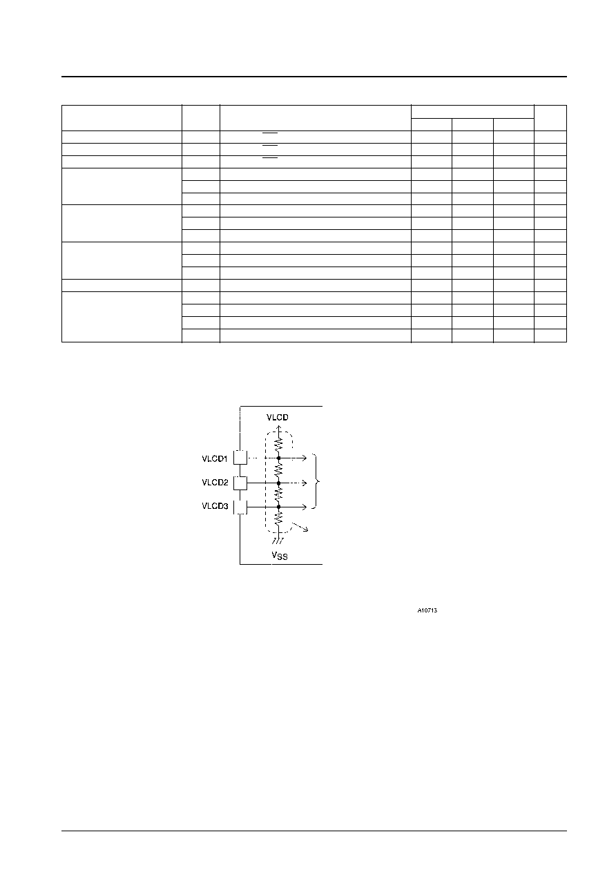
Electrical Characteristics
in the Allowable Operating Ranges
Note
*
1: Excluding the bias voltage generation divider resistor built into the V
LCD
1, V
LCD
2, and V
LCD
3. (See figure 1.)
Excluding these resistors
To the common and segment drivers
Figure 1