Overview
The LC75864E and LC75864W are 1/4 duty LCD display
drivers that can directly drive up to 96 segments and can
control up to four general-purpose output ports. These
products also incorporate a key scan circuit that accepts
input from up to 30 keys to reduce printed circuit board
wiring.
Features
∑ Key input function for up to 30 keys (A key scan is
performed only when a key is pressed.)
∑ 1/4 duty - 1/2 bias and 1/4 duty - 1/3 bias drive schemes
can be controlled from serial data (up to 96 segments).
∑ Sleep mode and all segments off functions that are
controlled from serial data
∑ Segment output port/general-purpose output port
function switching that is controlled from serial data
∑ Serial data I/O supports CCB format communication
with the system controller.
∑ Direct display of display data without the use of a
decoder provides high generality.
∑ Independent V
LCD
for the LCD driver block
(V
LCD
can be set to in the range V
DD
- 0.5 to 6.0 volts.)
∑ Provision of an on-chip voltage-detection type reset
circuit prevents incorrect displays.
∑ RC oscillator circuit
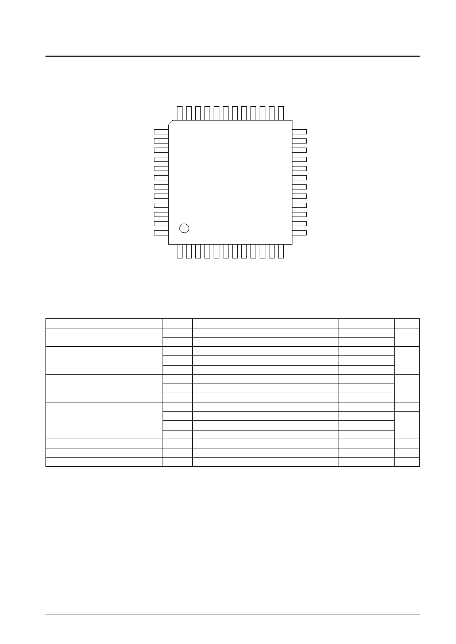
Package Dimensions
unit: mm
3156-QIP48E
Ordering number : ENN6860
D2501TN (OT) No. 6860-1/26
LC75864E, 75864W
SANYO Electric Co.,Ltd. Semiconductor Company
TOKYO OFFICE Tokyo Bldg., 1-10, 1 Chome, Ueno, Taito-ku, TOKYO, 110-8534 JAPAN
1/4 Duty LCD Display Drivers with Key Input Function
CMOS IC
Any and all SANYO products described or contained herein do not have specifications that can handle
applications that require extremely high levels of reliability, such as life-support systems, aircraft's
control systems, or other applications whose failure can be reasonably expected to result in serious
physical and/or material damage. Consult with your SANYO representative nearest you before using
any SANYO products described or contained herein in such applications.
SANYO assumes no responsibility for equipment failures that result from using products at values that
exceed, even momentarily, rated values (such as maximum ratings, operating condition ranges, or other
parameters) listed in products specifications of any and all SANYO products described or contained
herein.
unit: mm
3163A-SQFP48
0.5
7.0
9.0
0.15
0.18
0.75
0.5
0.75
0.75
0.5
0.75
0.5
0.1
1
12
13
24
25
36
37
48
7.0
9.0
1.7max
SANYO: SQFP48
[LC75864W]
∑ CCB is a trademark of SANYO ELECTRIC CO., LTD.
∑ CCB is SANYO's original bus format and all the bus
addresses are controlled by SANYO.
14.0
17.2
1.5
1.5
1.6
0.15
0.35
0.1
15.6
0.8
1.0
3.0max
1
48
12
13
24
25
36
37
2.7
14.0
17.2
1.5
1.5
1.6
1.0
[LC75864E]
SANYO: QIP48E
Allowable Operating Ranges
at Ta = ≠40 to +85∞C, V
SS
= 0 V
No. 6860-3/26
LC75864E, 75864W
Parameter
Symbol
Conditions
Ratings
Unit
min
typ
max
Supply voltage
V
DD
V
DD
4.5
6.0
V
V
LCD
V
LCD
V
DD
≠ 0.5
6.0
Input voltage
V
LCD
1
V
LCD
1
2/3 V
LCD
V
LCD
V
V
LCD
2
V
LCD
2
1/3 V
LCD
V
LCD
Input high level voltage
V
IH
1
CE, CL, DI
0.8 V
DD
6.0
V
V
IH
2
KI1 to KI5
0.6 V
DD
V
LCD
Input low level voltage
V
IL
CE, CL, DI, KI1 to KI5
0
0.2 V
DD
V
Recommended external
R
OSC
OSC
43
k
resistance
Recommended external
C
OSC
OSC
680
pF
capacitance
Guaranteed oscillation range
f
OSC
OSC
25
50
100
kHz
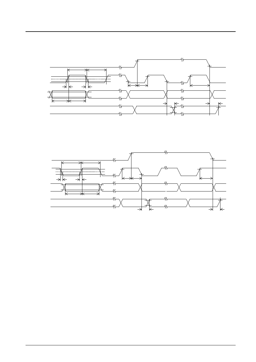
Data setup time
t
ds
CL, DI: Figure 2
160
ns
Data hold time
t
dh
CL, DI: Figure 2
160
ns
CE wait time
t
cp
CE, CL: Figure 2
160
ns
CE setup time
t
cs
CE, CL: Figure 2
160
ns
CE hold time
t
ch
CE, CL: Figure 2
160
ns
High level clock pulse width
t
¯H
CL: Figure 2
160
ns
Low level clock pulse width
t
¯L
CL: Figure 2
160
ns
Rise time
t
r
CE, CL, DI: Figure 2
160
ns
Fall time
t
f
CE, CL, DI: Figure 2
160
ns
DO output delay time
t
dc
DO, R
PU
= 4.7 k
, CL = 10 pF
*
1
: Figure 2
1.5
µs
DO rise time
t
dr
DO, R
PU
= 4.7 k
, CL = 10 pF
*
1
: Figure 2
1.5
µs
Note:
*
1. Since DO is an open-drain output, these times depend on the values of the pull-up resistor R
PU
and the load capacitance C
L
.
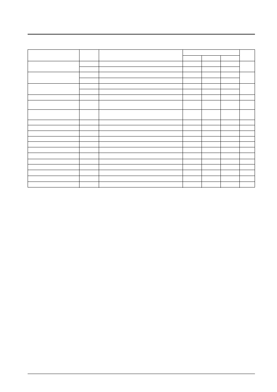
Electrical Characteristics
for the Allowable Operating Ranges
No. 6860-4/26
LC75864E, 75864W
Parameter
Symbol
Conditions
Ratings
Unit
min
typ
max
Hysteresis
V
H
CE, CL, DI, KI1 to KI5
0.1 V
DD
V
Power-down detection voltage
V
DET
2.5
3.0
3.5
V
Input high level current
I
IH
CE, CL, DI: V
I
= 6.0 V
5.0
µA
Input low level current
I
IL
CE, CL, DI: V
I
= 0 V
≠5.0
µA
Input floating voltage
V
IF
KI1 to KI5
0.05 V
DD
V
Pull-down resistance
R
PD
KI1 to KI5: V
DD
= 5.0 V
50
100
250
k
Output off leakage current
I
OFFH
DO: V
O
= 6.0 V
6.0
µA
V
OH
1
KS1 to KS6: I
O
= ≠500 µA
V
LCD
≠ 1.0
V
LCD
≠ 0.5
V
LCD
≠ 0.2
Output high level voltage
V
OH
2
P1 to P4: I
O
= ≠1 mA
V
LCD
≠ 1.0
V
V
OH
3
S1 to S24: I
O
= ≠20 µA
V
LCD
≠ 1.0
V
OH
4
COM1 to COM4: I
O
= ≠100 µA
V
LCD
≠ 1.0
V
OL
1
KS1 to KS6: I
O
= 25 µA
0.2
0.5
1.5
V
OL
2
P1 to P4: I
O
= 1 mA
1.0
Output low level voltage
V
OL
3
S1 to S24: I
O
= 20 µA
1.0
V
V
OL
4
COM1 to COM4: I
O
= 100 µA
1.0
V
OL
5
DO: I
O
= 1 mA
0.1
0.5
V
MID
1
COM1 to COM4: 1/2 bias, I
O
= ±100 µA
1/2 V
LCD
≠
1/2 V
LCD
+
1.0
1.0
V
MID
2
S1 to S24: 1/3 bias, I
O
= ±20 µA
2/3 V
LCD
≠
2/3 V
LCD
+
1.0
1.0
Output middle level voltage
*
2
V
MID
3
S1 to S24: 1/3 bias, I
O
= ±20 µA
1/3 V
LCD
≠
1/3 V
LCD
+
V
1.0
1.0
V
MID
4
COM1 to COM4: 1/3 bias, I
O
= ±100 µA
2/3 V
LCD
≠
2/3 V
LCD
+
1.0
1.0
V
MID
5
COM1 to COM4: 1/3 bias, I
O
= ±100 µA
1/3 V
LCD
≠
1/3 V
LCD
+
1.0
1.0
Oscillator frequency
f
OSC
OSC: R
OSC
= 43 k
, COSC = 680 pF
40
50
60
kHz
I
DD
1
V
DD
: Sleep mode
100
I
DD
2
V
DD
: V
DD
= 6.0 V, output open, f
OSC
= 50 kHz
270
540
Current drain
I
LCD
1
V
LCD
: Sleep mode
5
µA
I
LCD
2
V
LCD
: V
LCD
= 6.0 V, output open, 1/2 bias, f
OSC
= 50 kHz
100
200
I
LCD
3
V
LCD
: V
LCD
= 6.0 V, output open, 1/3 bias, f
OSC
= 50 kHz
60
120
Note:
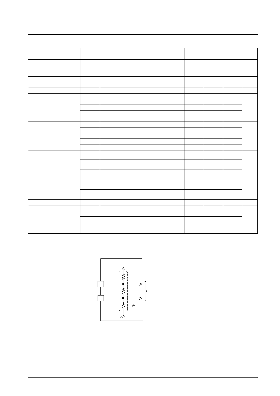
*
2. Excluding the bias voltage generation divider resistor built into V
LCD
1 and V
LCD
2. (See Figure 1.)
To the common segment driver
Excluding these resistors.
V
LCD
1
V
LCD
V
LCD
2
Figure 1