 | –≠–ª–µ–∫—Ç—Ä–æ–Ω–Ω—ã–π –∫–æ–º–ø–æ–Ω–µ–Ω—Ç: LC78213 | –°–∫–∞—á–∞—Ç—å:  PDF PDF  ZIP ZIP |
Applications
Function switching under serial data control in amplifiers,
receivers, and other electronic equipment
Features
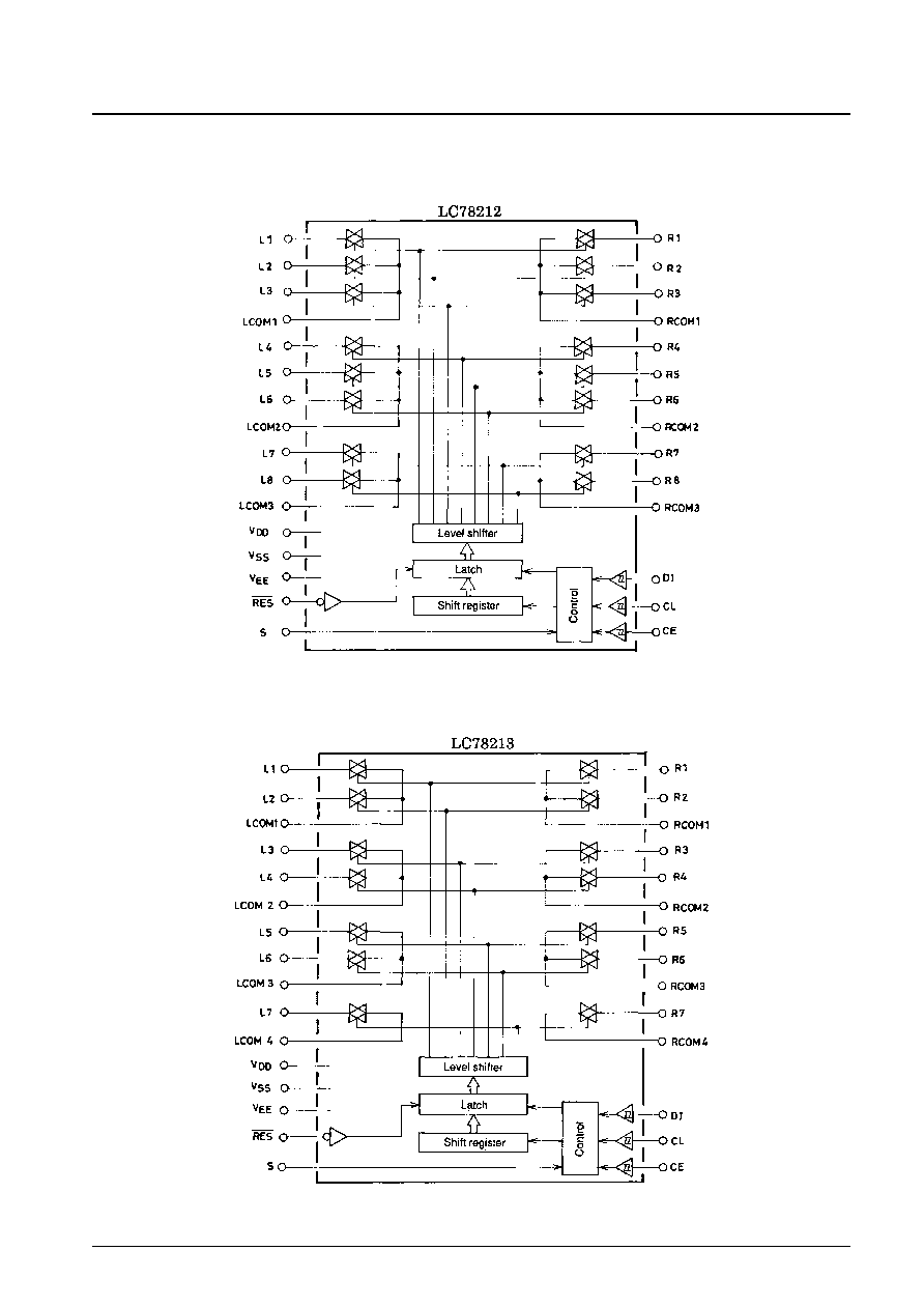
∑ Two sets of eight (or in the LC78213, seven) built-in
circuits with three switching configurations available
based on differing internal connections
∑ Control according to serial data sent from a micro-
processor, and easy connection to 5 V microprocessors
∑ Two identical products can be connected to a shared bus
due to the provision of a select pin (S).
∑ A reset pin that turns off all analog switches
∑ A ±20 V withstand voltage rating allows these products
to provide a wide dynamic range.
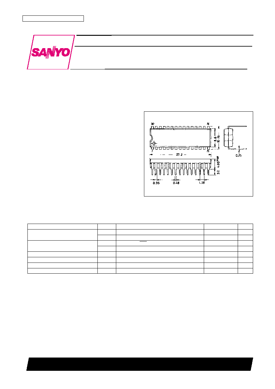
Package Dimensions
unit: mm
3061-DIP30S
CMOS LSI
Ordering number : EN4817A
73096HA (OT)/72994 TH (OT) No. 4817-1/6
SANYO: DIP30S
[LC78211, 78212, 78213]
SANYO Electric Co.,Ltd. Semiconductor Bussiness Headquarters
TOKYO OFFICE Tokyo Bldg., 1-10, 1 Chome, Ueno, Taito-ku, TOKYO, 110 JAPAN
Analog Function Switch
LC78211, 78212, 78213
Specifications
Absolute Maximum Ratings
at Ta = 25∞C
Parameter
Symbol
Conditions
Ratings
Unit
Maximum supply voltage
V
DD
max
V
DD
≠0.3 to +20
V
V
EE
max
V
EE
≠20 to +0.3
V
Maximum input voltage
V
I
1
DI, CL, CE, S, RES
≠0.3 to +20
V
V
I
2
L1 to L8, R1 to R8, LCOM1 to LCOM4, RCOM1 to RCOM4
V
EE
≠ 0.3 to V
DD
+ 0.3
V
Analog switch potential difference when on
V
ON
With the switch on
0.5
V
Allowable power dissipation
Pd max
Ta
75∞C
100
mW
Operating temperature range
Topr
≠30 to +75
∞C
Storage temperature range
Tstg
≠40 to +125
∞C

Pin Assignments
Allowable Operating Ranges
at Ta = 25∞C, V
SS
= 0 V,
|
V
DD
| |
V
EE
|
Note:
*
CE, CL and DI waveforms
No. 4817-2/6
LC78211, 78212, 78213
Parameter
Symbol
Conditions
min
typ
max
Unit
Maximum supply voltage
V
DD
V
DD
≠ V
EE
12 V: V
DD
6.0
18.5
V
V
EE
V
DD
≠ V
EE
12 V: V
EE
≠18.5
0
V
Input high level voltage
V
IH
1
DI, CL, CE
4.0
18.5
V
V
IH
2
S, RES
0.7 V
DD
V
DD
V
Input low level voltage
V
IL
1
DI, CL, CE
0
0.7
V
V
IL
2
S, RES
0
0.3 V
DD
V
Analog switch input
V
IN
L1 to L8, R1 to R8, LCOM1 to LCOM4,
V
EE
V
DD
V
voltage range
RCOM1 to RCOM4
Low level clock pulse width
t
¯L
CL
0.5
µs
High level clock pulse width
t
¯H
CL
0.5
µs
t
set up
CL, DI
0.5
µs
Setup time
t1
*
CL, CE
0.5
µs
t2
*
CL, CE
0.5
µs
t3
*
CL, CE
0.5
µs
Minimum reset pulse width
t
wRES
V
DD
6 V: RES
1.0
µs
Hysteresis
V
H
CL, CE, DI
0.3
V
Top view

Electrical Characteristics
at Ta = 25∞C, V
SS
= 0 V
Equivalent Circuit Block Diagrams
No. 4817-3/6
LC78211, 78212, 78213
Parameter
Symbol
Conditions
min
typ
max
Unit
I = 1 mA, V
DD
≠ V
EE
= 12 V:
R
ON
1
L1 to L8, R1 to R8, LCOM1 to LCOM4,
150
Analog switch on resistance
RCOM1 to RCOM4
I = 1 mA, V
DD
≠ V
EE
= 37 V:
R
ON
2
L1 to L8, R1 to R8, LCOM1 to LCOM4,
70
RCOM1 to RCOM4
V
IN
= 1 Vrms, f = 1 kHz, V
DD
≠ V
EE
= 37 V:
THD1
L1 to L8, R1 to R8, LCOM1 to LCOM4,
0.0015
0.01
%
Total harmonic distortion
RCOM1 to RCOM4
V
IN
= 0.1 Vrms, f = 1 kHz, V
DD
≠ V
EE
= 37 V:
THD2
L1 to L8, R1 to R8, LCOM1 to LCOM4,
0.01
0.05
%
RCOM1 to RCOM4
V
IN
= 0 dBV, f = 10 kHz, V
DD
≠ V
EE
= 37 V:
Feedthrough
F
TH
L1 to L8, R1 to R8, LCOM1 to LCOM4,
55
dB
RCOM1 to RCOM4
V
IN
= 0 dBV, f = 10 kHz, V
DD
≠ V
EE
= 37 V:
Crosstalk
CT
L1 to L8, R1 to R8, LCOM1 to LCOM4,
75
dB
RCOM1 to RCOM4
Input high level current
I
IH
V
I
= 18.5 V: DI, CL, CE, S, RES
+10
µA
Input low level current
I
IL
V
I
= 0 V: DI, CL, CE, S, RES
≠10
µA
Analog switch leakage current
V
I
= V
EE
to V
EE
+ 37 V:
(off state)
I
OFF
L1 to L8, R1 to R8, LCOM1 to LCOM4,
≠10
+10
µA
RCOM1 to RCOM4
Current drain
I
DD
V
DD
1.0
mA
Continued on next page.
Continued from preceding page.
No. 4817-4/6
LC78211, 78212, 78213
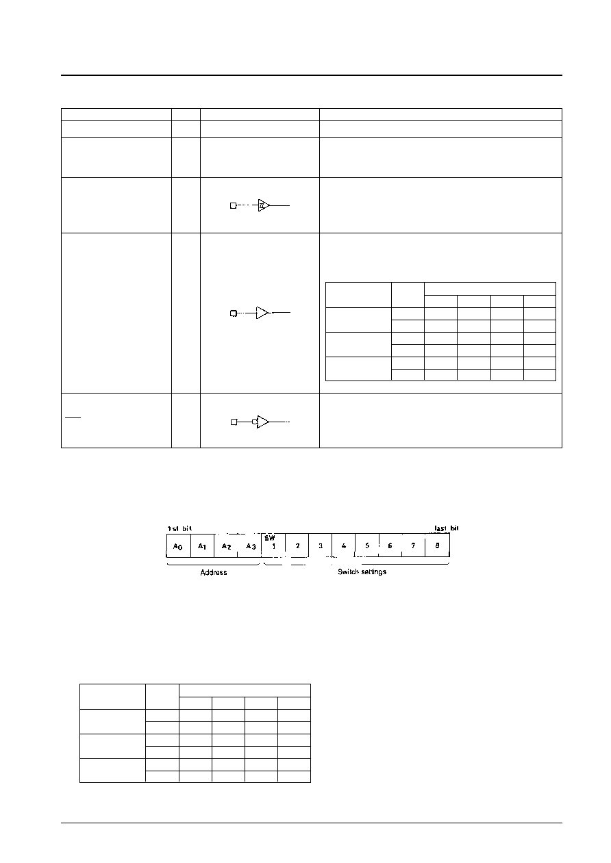
Pin Functions
Operation
1. Data Input Procedure
The LC78211, LC78212 and LC78213 are controlled by inputting specified data to the CL, DI and CE pins. The
input data consists of 12 bits, of which four bits are address and eight bits are data.
Bits correspond to the L1 to L8 and R1 to R8 analog switches, and a value of one turns the corresponding switch on,
and a value of zero turns it off.
0.........Off
1.........On
The address is used when the chip is connected to a shared bus. The data (address) that must be transmitted depends
on the S pin and the particular product as shown in the table below.
Note: The bit for switch eight in the LC78213 is a "don't care" bit, that is it can be either 0 or 1 without affecting
chip function. This is because the LC78213 has two sets of seven (not eight) circuits.
No. 4817-5/6
LC78211, 78212, 78213
Pin
I/O
Internal equivalent circuit
Pin function
V
DD
, V
SS
, V
EE
L1 to L8, R1 to R8,
LCOM1 to LCOM4,
RCOM1 to RCOM4
CL, DI, CE
S
RES
I
I
I
See the block diagram.
Power supply
Analog switch input and output
Serial data input (Schmitt buffer)
CL ..............Clock input
DI ...............Data input
CE .............Chip enable
Selection of one of two chips
The address is set to the values shown in the table below according to
the level input to the S pin.
Reset input
The states of the analog switches are undefined when power is first
applied. Setting this pin low will force all switches the off state.
Product
S pin
Address
level
A
0
A
1
A
2
A
3
LC78211
L
0
1
0
1
H
1
1
0
1
LC78212
L
0
0
1
1
H
1
0
1
1
LC78213
L
0
1
1
1
H
1
1
1
1
Product
S pin
Address
level
A
0
A
1
A
2
A
3
LC78211
L
0
1
0
1
H
1
1
0
1
LC78212
L
0
0
1
1
H
1
0
1
1
LC78213
L
0
1
1
1
H
1
1
1
1