 | –≠–ª–µ–∫—Ç—Ä–æ–Ω–Ω—ã–π –∫–æ–º–ø–æ–Ω–µ–Ω—Ç: LC7851 | –°–∫–∞—á–∞—Ç—å:  PDF PDF  ZIP ZIP |
Overview
The LC7851E demodulates the QPSK (quadrature phase
shift keying) modulated audio data broadcast by the
Japanese BS and CS broadcast satellites and converts that
data to an analog audio signal. This IC integrates on a
single chip the audio system signal processing required for
BS and CS receivers from QPSK demodulation to analog
audio reproduction. The main functions provided by the
LC7851E include QPSK demodulation, differential
decoding conversion, descrambling, deinterleaving, and
error correction. It also generates a PCM audio signal. The
PCM audio signal is converted to an analog audio signal
by on-chip digital filters and A/D converters.
Features
∑ QPSK demodulator, PCM decoder, digital filters, D/A
converters, and operational amplifiers integrated on a
single chip.
∑ The number of required external components has been
reduced and adjustment-free operation achieved in the
QPSK demodulator by implementing that block as a
digital circuit on a single chip.
∑ CPU interface using an I
2
C bus
∑ Interface circuits for CORTEC and SkyPort
descramblers
Functions
∑ QPSK demodulation
∑ Bit timing clock recovery
∑ Differential decoding conversion and parallel-to-serial
conversion
∑ Frame synchronization (forward protection: 8 cycles,
back protection: 3 cycles): Frame synchronized/not
synchronized detection flag output provided.
∑ Tenth-order M-series descrambling
∑ Deinterleaving
∑ BCH (63, 56) error correction and dual error detection:
Single error detected flag output provided.
∑ Support for both interpolation and previous data hold
when a dual error is detected.
Control bit majority judgment protection every 16
frames
∑ Register data previous value hold when dual errors are
detected using BCH(7,3)
∑ Ten to 14 bit expansion of audio data during A mode
broadcasts.
∑ Data protection using majority control for the upper bits
of the audio data during B mode broadcasts
∑ Full complement of muting functions
-- Audio suppression provided (bit 16 of the post-
majority decision control bits)
-- Non-audio signal suppression (bits 2 to 5 of the post-
majority decision control bits)
-- Forced muting
-- Muting when not synchronized
-- Muting when large numbers of errors are detected
(modifiable conditions)
-- Channel switching
-- Charged (pay-per-view) program flag muting
-- Mute detection output provided.
∑ General-purpose ports (2 input ports and 8 output ports)
∑ EIAJ digital audio interface output
∑ 8
◊
oversampling digital filters
∑ Multi-bit D/A converter (with built-in output operational
amplifiers)
∑ 5 V single-voltage power supply
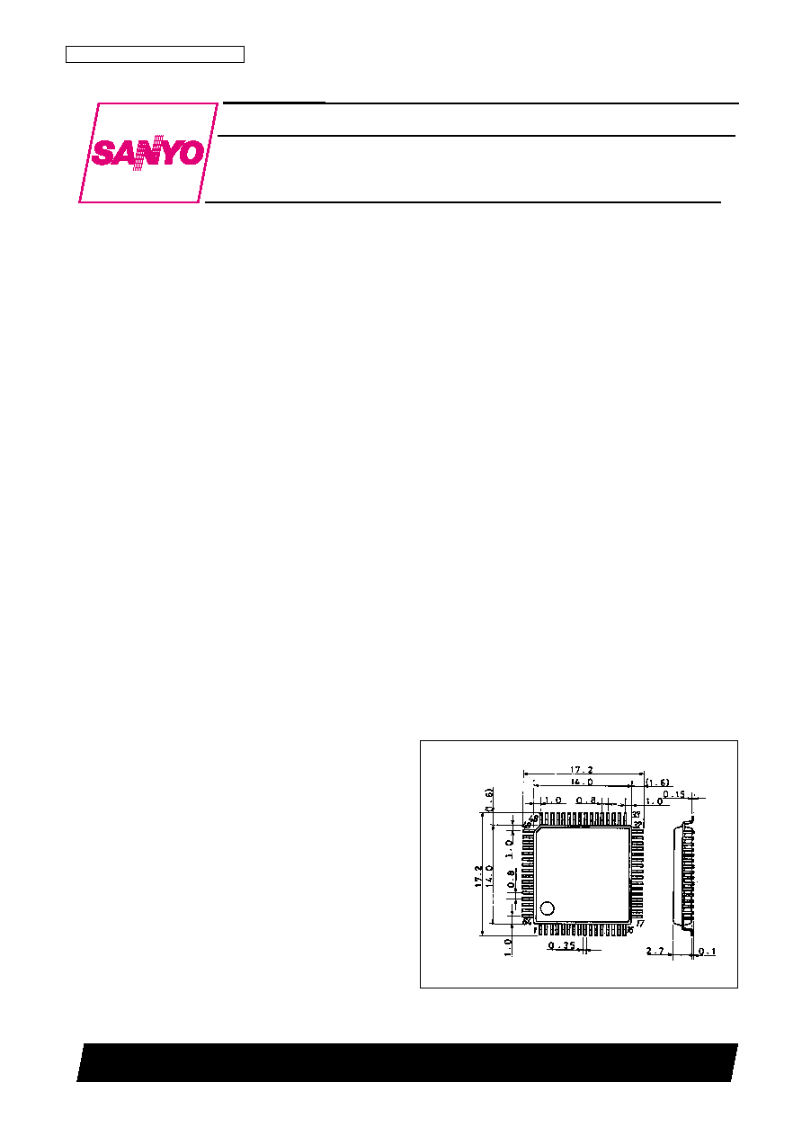
∑ QFP (QIP) 64E package
Package Dimensions
unit: mm
3195-QFP64E
CMOS LSI
Ordering number : EN5691
83097HA(OT) No. 5691-1/9
[LC7851E]
SANYO Electric Co.,Ltd. Semiconductor Bussiness Headquarters
TOKYO OFFICE Tokyo Bldg., 1-10, 1 Chome, Ueno, Taito-ku, TOKYO, 110 JAPAN
QPSK Demodulation and Audio Signal-Processing IC
for Satellite Broadcast Reception
LC7851E
SANYO: QIP64E
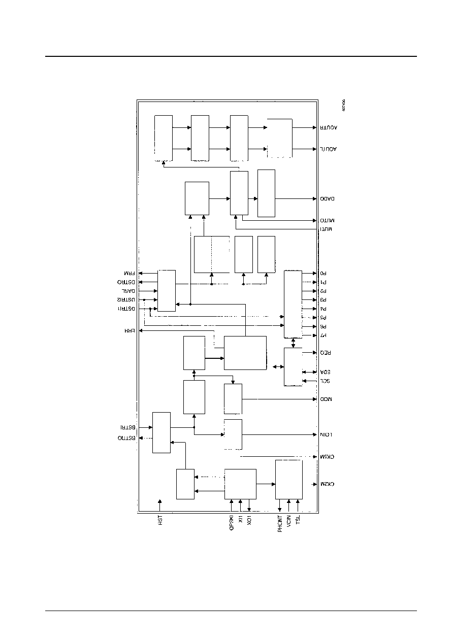
Block Diagram
No. 5691-2/9
LC7851E
Differential conversion
parallel-to-serial
converter
QPSK
demodulator
Scramble interface 1
Sync detection
and sync protection
Descrambler
Control bit extraction
CPU interface
Deinterleaving
Scramble interface 2
10 to 14 bits expansion
Data
interpolation and previous value hold
8
◊
oversampling digital filters
Digital de-emphasis
filter
D/A converter
Audio signal
buffer amplifier
Audio switching
Digital audio interface
output
Upper bit majority
protection
Range bit error
correction
For-fee flag detection
General-purpose ports
Error detection and correction
Bit timing clock
recovery
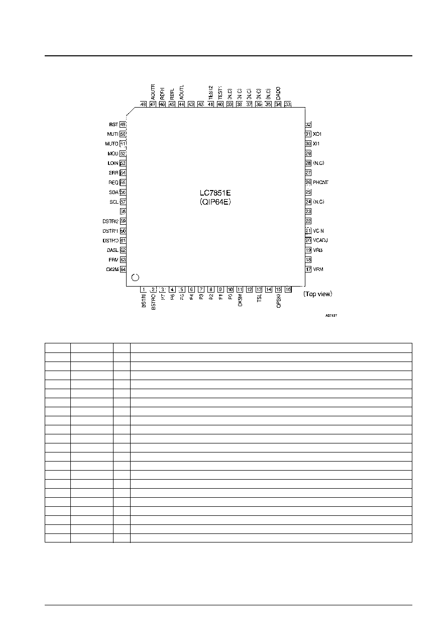
Pin Assignment
No. 5691-3/9
LC7851E
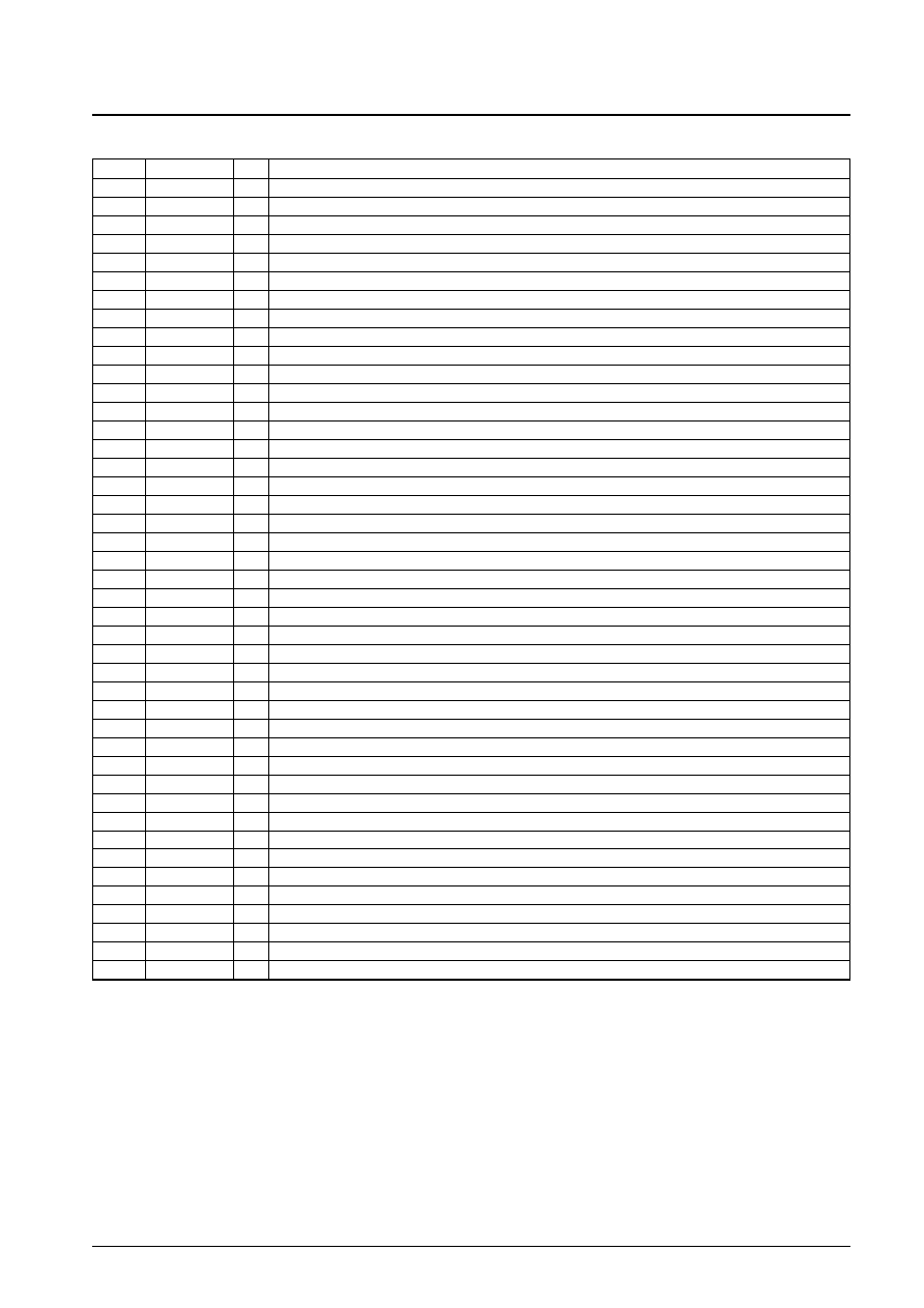
Pin Functions
Pin No.
Pin
I/O
Function
1
BSTRI
I
Bit stream input
2
BSTRO
O
Bit stream output
3
P7
O
General-purpose output port
4
P6
O
General-purpose output port
5
P5
O
General-purpose output port
6
P4
O
General-purpose output port
7
P3
O
General-purpose output port
8
P2
O
General-purpose output port
9
P1
O
General-purpose output port
10
P0
O
General-purpose output port
11
CK5M
O
Filter adjustment clock output (5.7272 MHz)
12
DV
DD
I
Digital system power supply
13
TSL
I
Output control for the state when reset by the PHCNT pin (Low: high-impedance, high: 50% duty pulse output)
14
AV
SS
I
Internal A/D converter ground
15
QPSKI
I
QPSK modulated signal input
16
AV
DD
I
Internal A/D converter power supply
17
VRM
O
Internal A/D converter reference (center) output
18
AV
SS
I
Internal A/D converter ground
19
VRB
O
Internal A/D converter reference (low) output
20
VCADJ
Connection for internal VCO adjustment external resistor
21
VCIN
I
Internal VCO control input
Continued on next page.
CV
DD
CV
SS
DV
SS
AV
DD
AV
SS
DV
DD
DV
SS
V
SS
V
DD
PV
SS
VV
SS
AV
SS
PV
DD
VV
DD
DV
DD
No. 5691-4/9
LC7851E
Continued from preceding page.
Pin No.
Pin
I/O
Function
22
VV
SS
I
Internal VCO ground
23
VV
DD
I
Internal VCO power supply
24
(N.C)
25
PV
DD
I
Phase comparator power supply
26
PHCNT
O
Phase comparator output
27
PV
SS
I
Phase comparator ground
28
(N.C)
29
V
DD
I
Oscillator circuit power supply
30
XI1
I
Crystal oscillator (22.909088 MHz) input
31
XO1
O
Crystal oscillator (22.909088 MHz) output
32
V
SS
I
Oscillator circuit ground
33
DV
SS
I
Digital system ground
34
DADO
O
Digital audio interface output
35
(N.C)
36
(N.C)
37
(N.C)
38
(N.C)
39
(N.C)
40
TEST1
I
Test pin
41
TEST2
I
Test pin
42
DV
DD
I
Digital system power supply
43
CV
SS
I
Internal D/A converter ground
44
AOUTL
O
Left channel audio data output
45
REFL
O
Internal D/A converter reference voltage: low
46
REFH
O
Internal D/A converter reference voltage: high
47
AOUTR
O
Right channel audio data output
48
CV
DD
I
Internal D/A converter power supply
49
RST
I
Reset input
50
MUTI
I
Forced muting input
51
MUTO
O
Mute detection output (When muting detected: high)
52
MOD
O
Audio mode detection output (A mode: low, B mode: high)
53
LOIN
O
Frame synchronization detection output (When synchronized: low)
54
ERR
O
Error detection output (Error detected: high)
55
REQ
O
Host CPU readout request signal
56
SDA
I/O
I
2
C bus data I/O
57
SCL
I
I
2
C bus clock input
58
DV
SS
I
Digital system ground
59
DSTRI2
I
Data stream input 2/general-purpose I/O port
60
DSTRI1
I
Data stream input 1/general-purpose I/O port
61
DSTRO
O
Data stream output (post-error correction data)
62
DASL
I
Descrambler interface switching
63
FRM
O
Frame synchronization signal
64
CK2M
O
Bit stream clock (2.048 MHz)
Caution: All NC pins must be left open.
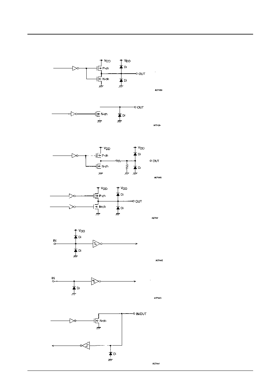
Pin Input and Output Circuit Diagrams
∑ Output pins (Output pins other than P0 to P7, SDA, PHCNT, CK5M, VRM, VRB, REFH, REFL, AOUTR, and
AOUTL)
∑ Output pins: P0 to P7
∑ Output pin: CK5M
∑ Output pin: PHCNT
∑ Input pins: SCL, DSTRI1, and DSTRI2
∑ I/O pin: SDA
No. 5691-5/9
LC7851E
∑ Input pins (Input pins other than QPSKI, SCL, SDA, DSTRI1, DSTRI2, and VCIN)
These are n-channel open drain outputs.