Ordering number : EN6021
D1898RM (OT) No. 6021-1/11
Overview
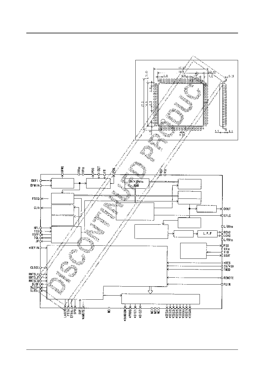
The LC78602NE CMOS IC implements compact disc
player signal processing, servo control, LED display, key
input acquisition, and remote controller processing
without requiring control by a separate microcontroller.
The basic functions provided include demodulation of the
EFM signal from the optical pickup, deinterleaving, error
detection and correction, 8
◊
oversampling digital filters,
D/A converter (with built-in analog low-pass filter), LED
driver, remote controller processing, key acquisition, and
control processing. Thus this IC can provide excellent
cost/performance characteristics when implementing a
low-end CD player.
Functions
∑ Implements CD play/pause, disc stop, track selection,
fast forward, reverse, repeat mode playback of 1 track or
the whole disc, programmed play (setup, play, and clear)
of up to 16 tracks, and random repeat play under the
control of key input or remote controller input.
<Signal-Processing Block>
∑ Slices an input high-frequency signal at an accurate
level, converts the EFM signal, and generates a clock
with an average frequency of 4.3218 MHz using a PLL
circuit that performs a phase comparison with an
internal VCO.
∑ Accurately generates not only the reference clock but
also all necessary internal timings using an external
16.9344MHz crystal.
∑ Controls the disc motor speed using a frame difference
signal created based on the reproduced clock signal and
a reference clock.
∑ Performs detection, protection, and interpolation for the
frame synchronizing signal to assure stable data readout.
∑ Demodulates the EFM signal, converting it to 8-bit
symbol data.
∑ Separates the subcode data from the EFM signal and
outputs that data to the internal control processing block.
∑ After applying a CRC check to the subcode Q signal,
outputs that signal to the internal control processing
block.
∑ Buffers the demodulated EFM signal data in internal
RAM and compensates for ±4 frames of jitter due to
disc speed fluctuations.
∑ Performs unscrambling and deinterleaving by reordering
the demodulated EFM signal data to the stipulated order.
∑ Performs error detection and correction and flag
processing (C1: dual errors, C2: dual errors)
∑ The C2 flags are set based on the C1 flags and the result
of the C2 processing, and the signal is interpolated or
previous value hold is applied based on the C2 flags.
Dual interpolation is adopted in the interpolation circuit.
Previous value hold is applied if two or more
consecutive errors are indicated by the C2 flags.
∑ Performs track jump, focus start, disc motor start/stop,
muting on/off, track count, and other operations under
control of the internal control processing block.
∑ Provides digital outputs.
∑ Generates D/A converter input signals with continuity
improved by 8
◊
oversampling digital filters.
∑ Includes on-chip third-order noise shaper delta-sigma
D/A converters with built-in analog low-pass filter.
∑ Digital deemphasis circuit
∑ Adopts zero-cross muting.
<Display Block>
∑ On-chip LED drivers for 7 segment 2-digit display plus
play, program, repeat, and random indicators
<Control Processing Block>
∑ Key matrix circuit with 1 input and 8 outputs for an
8-key matrix
∑ Supports remote controller input.
LC78602NE
SANYO Electric Co.,Ltd. Semiconductor Bussiness Headquarters
TOKYO OFFICE Tokyo Bldg., 1-10, 1 Chome, Ueno, Taito-ku, TOKYO, 110-8534 JAPAN
Compact Disc Player DSP with
Built-in Microcontroller
CMOS IC
Any and all SANYO products described or contained herein do not have specifications that can handle
applications that require extremely high levels of reliability, such as life-support systems, aircraft's
control systems, or other applications whose failure can be reasonably expected to result in serious
physical and/or material damage. Consult with your SANYO representative nearest you before using
any SANYO products described or contained herein in such applications.
SANYO assumes no responsibility for equipment failures that result from using products at values that
exceed, even momentarily, rated values (such as maximum ratings, operating condition ranges, or other
parameters) listed in products specifications of any and all SANYO products described or contained
herein.
No. 6021-4/11
LC78602NE
Parameter
Symbol
Applicable pins
Conditions
Ratings
Unit
min
typ
max
Current drain
I
DD
V
DD
, XV
DD
, L/RV
DD
, VV
DD
35
55
mA
DEFI, 3 V/
*
5 V, EFMIN, TMOD, HFL,
High-level input current
I
IH
1
TES, PUIN,
*
KEYIN, RMTSL1 to 3,
V
IN
= V
DD
5
µA
REMOTE, CLOSE,
*
RES, DRF
I
IH
2
LASER, FSTA, EFBAL, SP8
V
IN
= V
DD
250
500
1000
µA
DEFI, 3 V/
*
5 V, EFMIN, TMOD, HFL,
Low-level input current
I
IL
1
TES, RMTSL2 to 3, REMOTE,
*
RES, V
IN
= 0 V
≠5
µA
DRF
I
IL
2
PUIN,
*
KEYIN, RMTSL1, CLOSE
V
IN
= 0 V
≠25
≠50
≠100
µA
EFMO, CLV, TOFF, TGL, JP, LASER,
V
OH
1
FSTA, EFBAL, SP8, FSEQ, PCK,
I
OH
= ≠1 mA
0.8 V
DD
V
High-level output voltage
SLOF, SLED+, SLED≠, EFLG, FSX,
*
AMUTE
V
OH
4
DOUT
I
OH
= ≠12 mA
0.9 V
DD
V
EFMO, CLV, TOFF, TGL, JP, FSEQ,
V
OL
1
PCK, SLOF, SLED+, SLED≠, I
OL
= 1 mA
0.2 V
DD
V
Low-level output voltage
*
DIG1,
*
DIG2, EFLG, FSX,
*
AMUTE
V
OL
2
*
SEG1 to 8,
*
PROG,
*
RANDOM
I
OL
= 8 mA
0.2 V
DD
V
V
OL
5
DOUT
I
OL
= 12 mA
0.1 V
DD
V
Output off leakage current
I
OFFH
PDO, CLV, JP,
*
RANDOM
V
OUT
= V
DD
5
µA
I
OFFL
PDO, CLV, JP,
*
RANDOM
V
OUT
= 0 V
≠5
µA
R
PU
1
PUIN,
*
KEYIN, RMTSL1, CLOSE,
100
k
Pull-up resistance
*
DIG1,
*
DIG2,
*
PROG
R
PU
2
*
SEG1 to 8
50
k
Pull-down resistance
R
PD
LASER, FSTA, EFBAL, SP8
10
k
Charge pump output current
I
PDOH
PDO
R
ISET
= 68 k
64
80
96
µA
I
PDOL
PDO
R
ISET
= 68 k
≠96
≠80
≠64
µA
Electrical Characteristics
at Ta = ≠20 to +75∞C, V
DD
= 4.5 to 5.5 V, V
SS
= 0 V
Parameter
Symbol
Applicable pins
Conditions
Ratings
Unit
min
typ
max
Total harmonic distortion
THD+N
LCHO, RCHO
1 kHz: 0dB data input
0.025
0.04
%
20kHz low-pass filter used (built-in AD725D)
Dynamic range
DR
LCHO, RCHO
1 kHz: ≠60dB data input
86
88
dB
20kHz low-pass filter and A filter used (built-in AD725D)
Signal-to-noise ratio
S/N
LCHO, RCHO
1 kHz: 0dB data input
90
92
dB
20kHz low-pass filter and A filter used (built-in AD725D)
Crosstalk
CT
LCHO, RCHO
1 kHz: 0dB data input
80
82
dB
20kHz low-pass filter used (built-in AD725D)
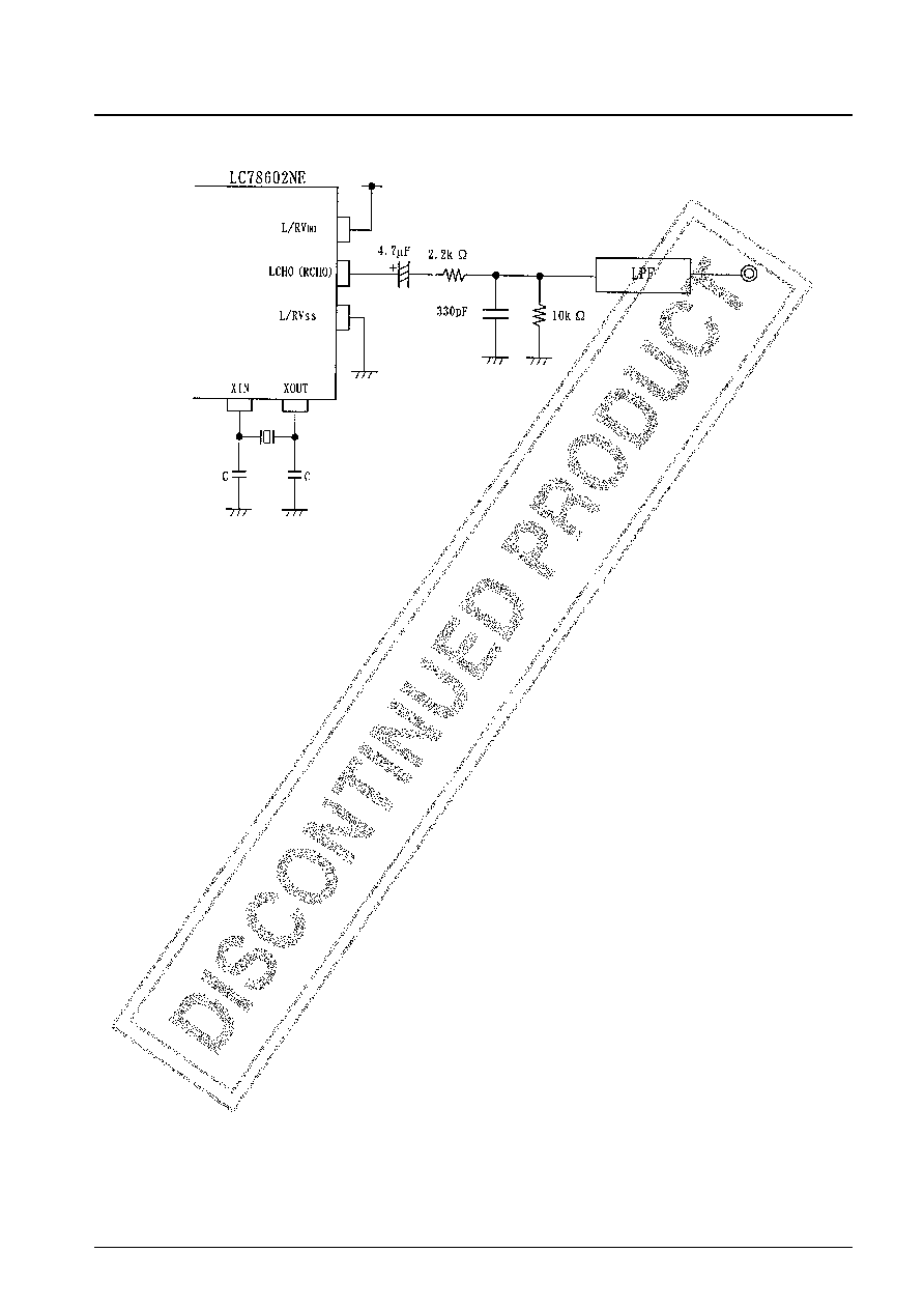
1-Bit D/A Converter Analog Characteristics
at Ta = 25∞C, V
DD
= L/RV
DD
= 5 V, V
SS
= L/RV
SS
= 0 V
Note: Measured in normal speed playback mode with the Sanyo 1-bit D/A converter block reference circuit.