 | –≠–ª–µ–∫—Ç—Ä–æ–Ω–Ω—ã–π –∫–æ–º–ø–æ–Ω–µ–Ω—Ç: LC78626E | –°–∫–∞—á–∞—Ç—å:  PDF PDF  ZIP ZIP |

Overview
The LC78626E is a monolithic compact disk player signal
processing and servo control CMOS IC equipped with an
internal anti-shock control function. Designed for total
functionality including support for EFM-PLL, and one-bit
D/A converter, and containing analog low-pass filter, the
LC78626E provides optimal cost-performance for low-end
CD players that provide anti-shock systems. The basic
functions provided by this IC include modulation of the
EFM signal from the optical pick-up, deinterleaving,
detection and correction of signal errors, prevention of a
maximum of approximately 10 seconds of skipping, signal
processing such as digital filtering (which is useful in
reducing the cost of the player), and processing of a
variety of servo-related commands from the
microprocessor.
Functions
∑ When an HF signal is input, it is sliced to precise levels
and converted to an EFM signal. The phase is compared
with the internal VCO and a PLL clock is reproduced at
an average frequency of 4.3218 MHz.
∑ Precise timing for a variety of required internal timing
needs (including the generation of the reference clock) is
produced by the attachment of an external 16.9344 MHz
crystal oscillator.
∑ The speed of revolution of the disk motor is controlled
by the frame phase difference signal generated by the
playback clock and the reference clock.
∑ The frame synchronizing signal is detected, stored, and
interpolated to insure stable data read back.
∑ The EFM signal is demodulated and converted to 8-bit
symbolic data.
∑ The demodulated EFM signal is divided into subcodes
and output to the external microprocessor. (Three
general I/O ports are shared [exclusively] for this
purpose.)
∑ After the subcode Q signal passes the CRC check, it is
output to the microprocessor through a serial
transmission (LSB first).
∑ The demodulated EFM signal is buffered in the internal
RAM, which is able to absorb ± 4 frame's worth of jitter
resulting from variations in the disk rotation speed.
∑ The demodulated EFM signal is unscrambled to a
specific sequence, and deinterleaving is performed.
∑ Error detection and correction is performed, as is a flag
process. (C1: two error/C2: two error correction
method.)
∑ The C2 flag is set after referencing the C1 flag and the
results of the C2 check, where the signal from the C2
flag is interpolated or held at its previous level. The
interpolation circuit uses double interpolation. When
there are two or more C2 flags in a row, the previous
value is held.
Package Dimensions
unit: mm
3151-QFP100E (FLP100)
CMOS LSI
13098HA(OT) No. 5692-1/32
SANYO: QIP100E (FLP100)
[LC78626E]
SANYO Electric Co.,Ltd. Semiconductor Bussiness Headquarters
TOKYO OFFICE Tokyo Bldg., 1-10, 1 Chome, Ueno, Taito-ku, TOKYO, 110-0005 JAPAN
DSP for Compact Disk Players
LC78626E
Ordering number : EN5692
Continued on next page.

No. 5692-2/32
LC78626E
Continued from preceding page.
∑ Command (such as track jump, start focus, disk motor
start/stop, muting on/off, track count, etc.) is are
executed after they are entered from the microprocessor.
(An 8-bit serial input is used.)
∑ The digital output is equipped internally.
∑ High speed access is supported through discretionary
track counting.
∑ Using the 4
◊
oversampling digital filter, D/A converter
signals with improved continuity of output data are
produced.
∑ A
-type D/A converter using a 3-order noise shaper is
equipped internally. (An analog low-pass filter is
equipped internally.)
∑ Internal digital attenuator (8-bit-[ALPHA]; 239 steps.)
∑ Internal digital deemphasis.
∑ Uses 0 cross mute.
∑ Bilingual compatibility.
∑ General I/O ports: 4. (Three of these are shared,
exclusively, with the subcode output function.)
∑ Up to ten seconds of skip prevention (when using 4M of
DRAM) through ADPCM compression/decompression
processing. 1M/4M bit DRAM can be selected.
∑ Memory overflow detection output.
∑ Free memory output.
Features
∑ 100-pin QFP
∑ A single 3.2 V/5 V power supply
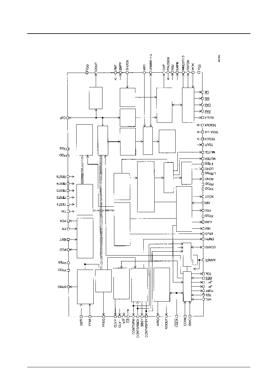
Equivalent Circuit Block Diagram
No. 5692-3/32
LC78626E
Digital out
RAM address
generator
Interpolation mute
Shock
detector
Contact
detector
ADPCM
encoder
Data width
changer
2K
◊
8-bit RAM
Digital
attenuator
4
◊
oversampling digital filter
C1, C2 error detection and
correction flag process
VCO clock production
clock control
Slice level control
Sync detect
EFM
demodulation
CLV digital servo
Subcode partition
QCRC
Microprocessor
interface
Servo commands
General ports
Disable
Crystal oscillator-system
timing generator
One-bit DAC
Low-pass
filter
ADPCM
decoder
DRAM control
Overflow process
initiation control

Pin Assignment
No. 5692-4/32
LC78626E
Top view

No. 5692-5/32
LC78626E
Parameter
Symbol
Conditions
Ratings
Unit
Maximum power supply voltage
V
DD
max
V
SS
≠0.3 to V
SS
+7.0
V
Input voltage
V
IN
V
SS
≠0.3 to V
DD
+0.3
V
Output voltage
V
OUT
V
SS
≠0.3 to V
DD
+0.3
V
Allowable power dissipation
Pd max
400
mW
Operating temperature range
Topr
≠20 to +75
∞C
Storage temperature range
Tstg
≠40 to +125
∞C
Specifications
Absolute Maximum Ratings
at Ta = 25∞C, V
SS
= 0V
Parameter
Symbol
Conditions
Ratings
Unit
min
typ
max
V
DD
1
V
DD
, XV
DD
, LV
DD
, RV
DD
, VV
DD
:
3.0
5.5
V
Power supply voltage
ATT/DF/DAC to the normal speed
V
DD
2
V
DD
, XV
DD
, LV
DD
, RV
DD
, VV
DD
:
3.6
5.5
V
All functions guaranteed to 2
◊
speed
V
IH
1
I/O and input pins with the exception of
0.7V
DD
V
DD
V
Input high level voltage
EFMI and DRAM0 to DRAM3
V
IH
2
EFMI
0.6V
DD
V
DD
V
V
IH
3
DRAM0 to DRAM3
0.45V
DD
V
DD
V
V
IL
1
I/O and input pins with the exception of
0
0.3V
DD
V
Input low level voltage
EFMI and DRAM0 to DRAM3
V
IL
2
EFMI
0
0.4V
DD
V
V
IL
2
DRAM0 to DRAM3
0
0.2V
DD
V
Data setup time
t
SU
COIN, RWC: Figure 1
400
ns
Data hold time
t
HD
COIN, RWC: Figure 1
400
ns
High level clock pulse width
t
WH
SBCK, CQCK: Figures 1 to 3
400
ns
Low level clock pulse width
t
WL
SBCK, CQCK: Figures 1 to 3
400
ns
Data read access time
t
RAC
SQOUT, PW: Figures 2 and 3
0
400
ns
Command transfer time
t
RWC
RWC: Figure 1
1000
ns
Subcode Q read enable time
t
SQE
WRQ: Figure 2, no RWC signal
11.2
ms
Subcode ready cycle time
t
SC
SFSY: Figure 3
136
µs
Subcode read enable time
t
SE
SFSY: Figure 3
400
µs
Port input data setup time
t
CSU
CONT2 to CONT5, RWC: Figure 4
400
ns
Port input data hold time
t
CHD
CONT2 to CONT5, RWC: Figure 4
400
ns
Port input clock setup time
t
RCQ
RWC, CQCK: Figure 4
100
ns
Port output data delay time
t
CDD
CONT2 TO CONT5, RWC: Figure 5
1200
ns
Input level
V
IN
1
EFMI: slice level control, V
DD
= 3.0 V
0.8
Vp-p
V
IN
2
XIN: C coupling input
1.0
Vp-p
Range of operating frequencies
f
OP
EFMI
10
MHz
Crystal oscillator frequency
f
X
XIN, XOUT
16.9344
MHz
Allowable Operating Range
at Ta = 25∞C, V
SS
= 0V
Parameter
Symbol
Conditions
Ratings
Unit
min
typ
max
Consumption current
I
DD
V
DD
, XV
DD
, LV
DD
, RV
DD
, VV
DD
:
14
20
mA
V
DD
= 3.0 to 3.4 V with normal playback
DEFI, EFMI, HFL, TES, RWC, COIN, CQCK,
I
IH
1
FMT, MR1, RES, TESD, WOK, PAUSE IN,
5
µA
SHOCK, TESCLK, TESA, TESB, TESC,
Input high level current.
TESGB, TEST1: V
IN
= V
DD
I
IH
2
TAI, TEST2 to TEST5, CS, TESE:
15
55
µA
V
IN
= V
DD
= 3.4 V
Electrical Characteristics
at Ta = 25∞C, V
DD
= 3.2 V V
SS
= 0V
Continued on next page.