20703RM(OT) No.7350-1/21
Any and all SANYO products described or contained herein do not have specifications that can handle
applications that require extremely high levels of reliability, such as life-support systems, aircraft's control
systems, or other applications whose failure can be reasonably expected to result in serious physical
and/or material damage. Consult with your SANYO representative nearest you before using any SANYO
products described or contained herein in such applications.
SANYO assumes no responsibility for equipment failures that result from using products at values that
exceed, even momentarily, rated values (such as maximum ratings, operating condition ranges, or other
parameters) listed in products specifications of any and all SANYO products described or contained
herein.
CMOS IC
Overview
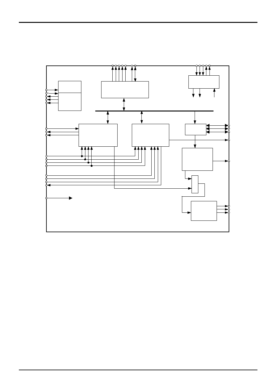
The LC78684E integrates, on a single chip, CD-ROM
signal-processing functions, MP3 signal-processing func-
tions, and CD-DA shockproof signal-processing functions.
The LC78684E achieves significant power savings by
implementing signal-processing functions using hard-
wired structures.
A CD player that supports playback of MPEG audio
(MP3) recorded on CD media as well as CD-DA
shockproof playback can be implemented by combining
this IC with a CD DSP, DRAM, and audio D/A converter,
and other circuits.
Features
MP3 Decoding Functions (MPEG audio standard
[ISO/IEC 11172-3] layer 3)
Decodes to a digital audio signal MP3 data decoded
by the CD-ROM decoder and outputs that audio
signal.
Supports all bit rates, including variable bit rate
operation.
Supports the following sampling rates.
MPEG1 (Fs = 32 K, 44.1 K, 48 K)
MPEG2 (Fs = 16 K, 22.05 K, 24 K)
MPEG2.5 (Fs = 8 K, 11.025 K, 12 K)
Can read out the MPEG header and ancillary data.
Automatically mutes the signal on CRC errors using
an MP3 CRC check function.
External MPEG serial data input function supports
memory card playback.
CD-ROM Decoding Functions
Supports CD-ROM modes 1 and 2 (forms 1 and 2)
Faithfully reproduces data stored on CD-ROM discs
using CD-ROM error correction functions.
Header and sector management
Supports playback speeds up to 4�.
In addition to data buffering also supports C2 error
flag buffering.
Provides external serial output of decoded CD-ROM
data.
CD-DA Playback Functions (Shockproof support)
Shockproof operation for about 180 seconds (com-
pressed mode) when 64M DRAM is used.
Shockproof function supports compressed, uncom-
pressed, and data through modes.
VCEC (variable speed) supports up to 4�-speed play-
back.
Audio Signal Processing
Serial audio signal output using LRCK, BCK, and
DATA signals.
(I�S format, either 16-bit or 20-bit precision PCM
output, data-slot supports 16-bit, 24-bit, and 32-bit
modes)
Digital bass boost function (4 modes), attenuator
function, and muting (
, 12 dB)
Provides a base clock (384 fs) output pin for use with
external digital filters and D/A converters.
DRAM Interface
Supports the use of from 1M to 64M of external
DRAM (EDO, 2CAS, 16-bit data bus memory)
Supports allocation of a user area in DRAM during
CD-ROM (MP3) playback.
Continued on next page.
MP3 Decoder for Compact Disc Players
LC78684E
Ordering number : ENN7350
LC78684E
No.7350-2/21
Continued from preceding page.
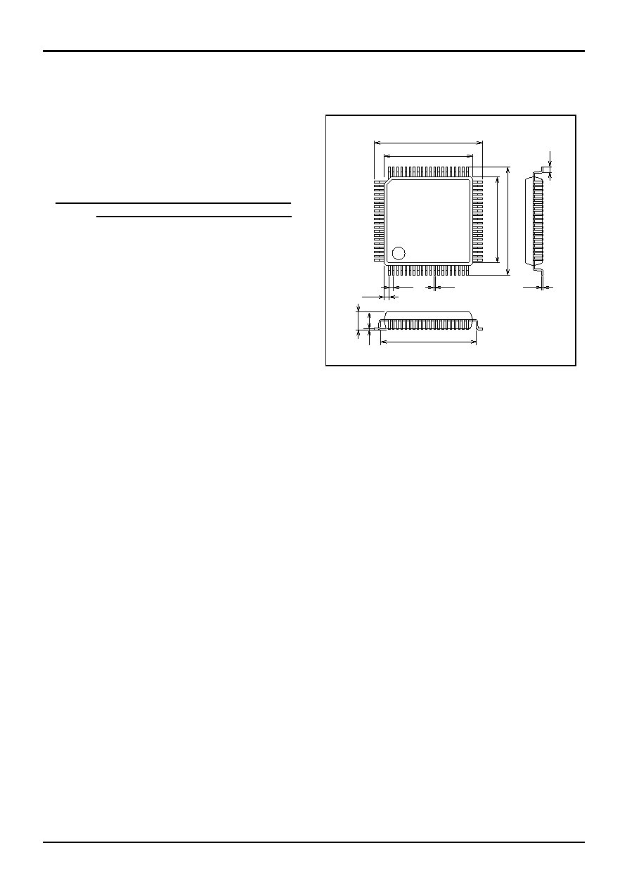
Package and Power Supply Voltage Specifications
Package: Sanyo QFP80 (14 � 14) (unit: mm)
Supply voltage
Internal power supply: 1.8 V (typical)
I/O power supply: 3.3 V (typical)
Analog system power supply: 3.3 V (typical)
MPEG Layer3 audio coding technology licensed from
Fraunhofer IIS and THOMSON multimedia
Package Dimensions
Unit: mm
3255-QFP80 (14 14)
[LC78684E]
14.0
14.0
17.2
17.2
0.15
0.1
3.0max
0.25
0.65
(0.83)
(2.7)
0.8
1
20
21
40
41
60
80
61
15.6
SANYO: SFP80
LC78684E
No.7350-5/21
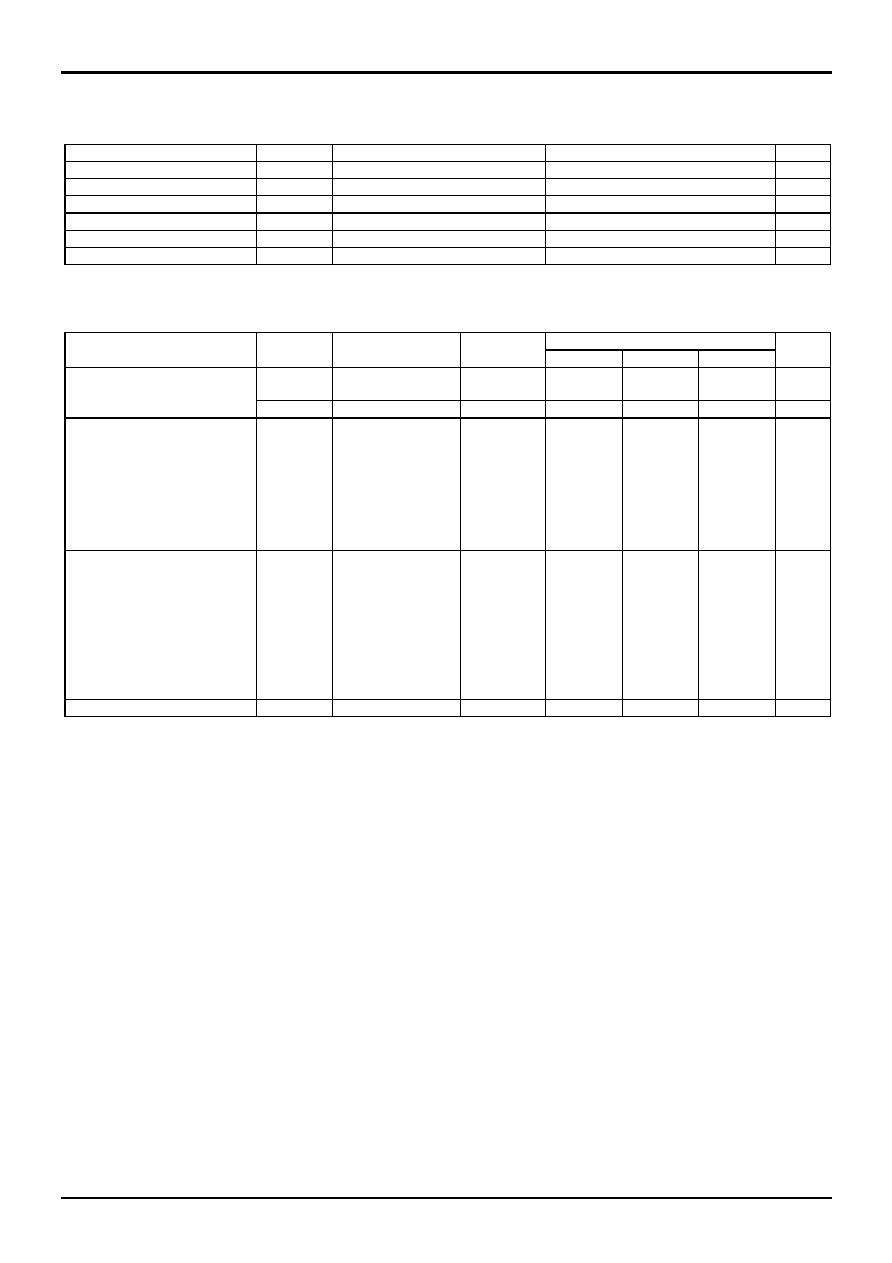
Pin Functions
Absolute Maximum Ratings at V
SS
0 V, AV
SS
0 V
Parameter
Symbol
Conditions
Ratings
Unit
Maximum supply voltage
V
DD
max
0.3 to V
SS
4.0
V
Input voltage
V
IN
0.3 to V
DD
1 0.3
V
Output voltage
V
OUT
0.3 to V
DD
1 0.3
V
Allowable power dissipation
Pdmax
400
mW
Operating temperature
Topr
30 to 75
C
Storage temperature
Tstg
40 to 125
C
Allowable Operating Ranges at Ta 30 to 75 C, V
SS
0 V, AV
SS
0V
Ratings
Parameter
Symbol
Pin name
Conditions
min
typ
max
Unit
V
DD
1
DV
DD
1, DV
DD
3,
DV
DD
4, DV
DD
6, AV
DD
3.0
3.3
3.6
V
Supply voltage
V
DD
2
DV
DD
2, DV
DD
5
1.62
1.8
1.98
V
High-level input voltage
V
IH
MDATA0 to 15,
LRSY, DATAIN,
DATACK, C2FIN,
PW, SBSY, SFSY,
STREQ, STCK,
STDAT, WOK,
CKIN, CE, CL,
CMDIN, RESB
0.8 V
DD
1
V
DD
1
V
Low-level input voltage
V
IL
MDATA0 to 15,
LRSY, DATAIN,
DATACK, C2FIN,
PW, SBSY, SFSY,
STREQ, STCK,
STDAT, WOK,
CKIN, CE, CL,
CMDIN, RESB,
TEST1, TEST2
0
0.2 V
DD
1
V
Operating frequency range
Fop
CKIN
16.9344
MHz