 | –≠–ª–µ–∫—Ç—Ä–æ–Ω–Ω—ã–π –∫–æ–º–ø–æ–Ω–µ–Ω—Ç: LC78833V | –°–∫–∞—á–∞—Ç—å:  PDF PDF  ZIP ZIP |
Ordering number : EN
*
5212
D3095HA (OT) No. 5212-1/11
Overview
The LC78833M and LC78833V are CMOS 16-bit D/A
converters with built-in 4
◊
oversampling digital filters.
Functions and Features
[Digital Filter Block]
∑ 4
◊
oversampling filters: Two FIR filter stages (33rd and
ninth order)
∑ De-emphasis filter: Supports a 44.1 kHz sampling
frequency (fs).
[D/A Converter Block]
∑ Dynamic level shifting conversion 16-bit D/A converter
∑ D/A converters for two channels (synchronized outputs)
on a single chip
∑ On-chip output operational amplifiers
∑ System clock: 384fs
∑ 5-V single-voltage power supply
∑ Supports low-voltage operation (3.0 V)
∑ Implemented in a Si gate CMOS process for low power.
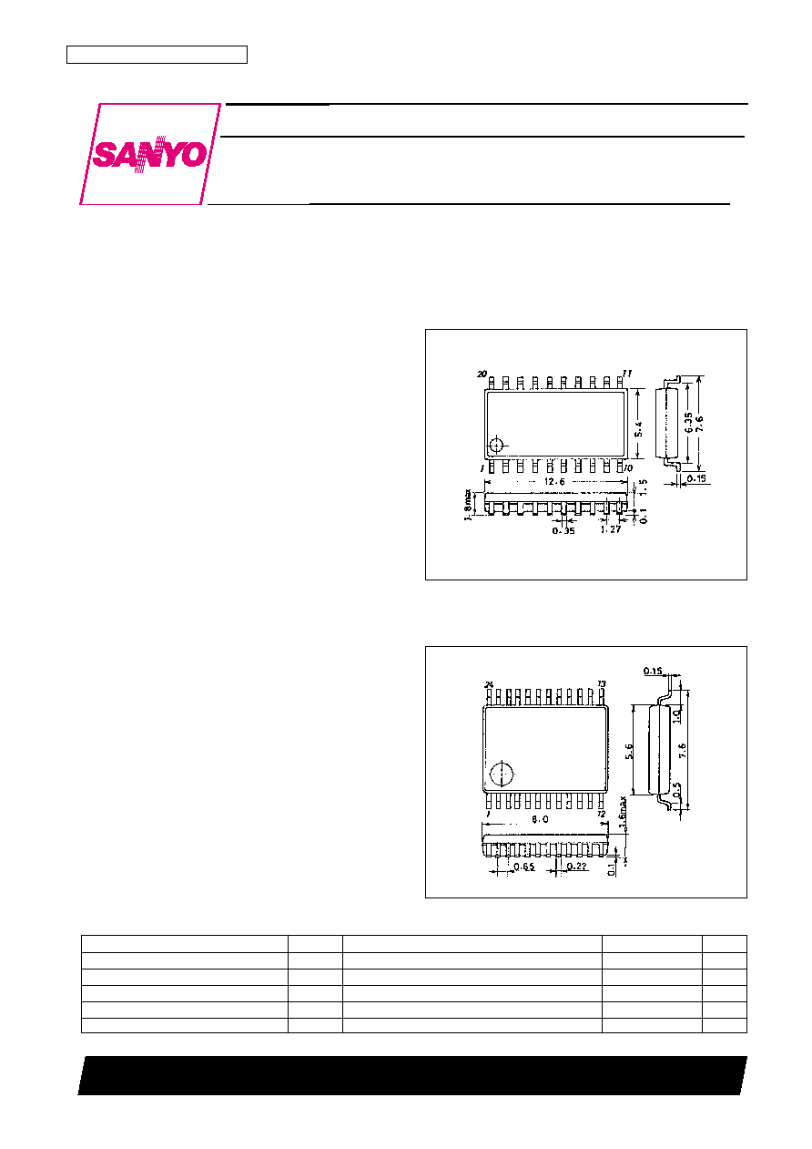
Package Dimensions
unit: mm
3036B-MFP20
unit: mm
3175A-SSOP24
Preliminary
SANYO: MFP20
[LC78833M]
SANYO: SSOP24
[LC78833V]
LC78833M, 78833V
SANYO Electric Co.,Ltd. Semiconductor Bussiness Headquarters
TOKYO OFFICE Tokyo Bldg., 1-10, 1 Chome, Ueno, Taito-ku, TOKYO, 110-8534 JAPAN
Digital Audio 16-Bit D/A Converter
with Built-In Digital Filters
CMOS LSI
Specifications
Absolute Maximum Ratings
at Ta = 25∞C, V
SS
= 0 V
Parameter
Symbol
Conditions
Ratings
Unit
Maximum supply voltage
V
DD
max
≠0.3 to +7.0
V
Maximum input voltage
V
IN
max
≠0.3 to V
DD
+ 0.3
V
Maximum output voltage
V
OUT
max
≠0.3 to V
DD
+ 0.3
V
Operating temperature
Topr
≠30 to +75
∞C
Storage temperature
Tstg
≠40 to +125
∞C
Allowable Operating Ranges
Electrical Characteristics (1)
at Ta = 25∞C, AV
DD
= DV
DD
= Vref H = 5.0 V, AGND = DGND = Vref L = 0 V, unless otherwise specified
Note: 1. Here, 0 dB means full scale.
2. Pin numbers in parentheses are for the LC78833V.
Electrical Characteristics (2)
at Ta = 25∞C, AV
DD
= DV
DD
= Vref H = 3.0 V, AGND = DGND = Vref H = 0 V, unless otherwise specified
Note: 1. Here, 0 dB means full scale.
2. Pin numbers in parentheses are for the LC78833V.
No. 5212-2/11
LC78833M, 78833V
Parameter
Symbol
Conditions
min
typ
max
Unit
Supply voltage
V
DD
3.0
5.0
5.5
V
Reference voltage (high)
Vref H
V
DD
≠ 0.3
V
DD
V
Reference voltage (low)
Vref L
0
+0.3
V
Parameter
Symbol
Conditions
min
typ
max
Unit
D/A converter resolution
RES
16
Bit
Total harmonic distortion
THD
At 1 kHz and 0 dB
*
1
0.08
%
Dynamic range
DR
At 1 kHz, ≠60 dB
92
94
dB
Crosstalk
CT
At 1 kHz and 0 dB
≠85
dB
Signal-to-noise ratio
S/N
JIS-A
96
100
dB
Full-scale output voltage
VFS
2.6
2.8
3.0
Vp-p
Power dissipation
Pd
At fs = 44.1 kHz
60
90
mW
Output load resistance
RL
Pins 1 and 20 (1 and 24)
*
2
5
k
Parameter
Symbol
Conditions
min
typ
max
Unit
D/A converter resolution
RES
16
Bit
Total harmonic distortion
THD
At 1 kHz and 0 dB
*
1
0.10
%
Dynamic range
DR
At 1 kHz, ≠60 dB
90
92
dB
Crosstalk
CT
At 1 kHz and 0 dB
≠85
dB
Signal-to-noise ratio
S/N
JIS-A
94
98
dB
Full-scale output voltage
VFS
1.55
1.7
1.85
Vp-p
Power dissipation
Pd
At fs = 44.1 kHz
15
25
mW
Output load resistance
RL
Pins 1 and 20 (1 and 24)
*
2
30
k
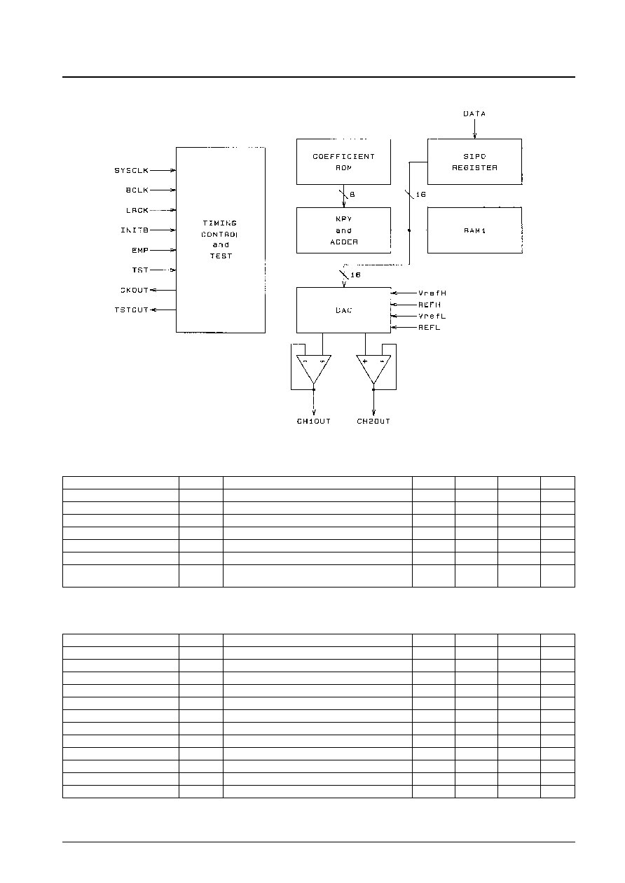
Block Diagram
DC characteristics
at Ta = ≠30 to 75∞C, V
DD
= 3.0 to 5.5 V, V
SS
= 0 V
Note:
*
Pins in parentheses apply to the LC78833V.
AC Characteristics
at Ta = ≠30 to 75∞C, V
DD
= 3.0 to 5.5 V, V
SS
= 0 V
No. 5212-3/11
LC78833M, 78833V
Parameter
Symbol
Conditions
min
typ
max
Unit
Input high-level voltage (1)
V
IH
1
Pins 5, 6, 7, 12, 13, and 14 (pins 6, 7, 8, 14, 16, and 17)
*
2.2
V
Input low-level voltage (1)
V
IL
1
Pins 5, 6, 7, 12, 13, and 14 (pins 6, 7, 8, 14, 16, and 17)
*
0.8
V
Input high-level voltage (2)
V
IH
2
Pin 8 (pin 9)
*
0.7 V
DD
V
Input low-level voltage (2)
V
IL
2
Pin 8 (pin 9)
*
0.3 V
DD
V
Output high-level voltage
V
OH
Pin 9 (pin 11)
*
: I
OH
= ≠3 mA
2.4
V
Output low-level voltage
V
OL
Pin 9 (pin 11)
*
: I
OL
= 3 mA
0.4
V
Input leakage current
I
L
Pins 5, 6, 7, 8, 12, 13, and 14
≠25
+25
µA
(pins 6, 7, 8, 9, 14, 16, and 17)
*
: V
I
= V
SS
, V
DD
Parameter
Symbol
Conditions
min
typ
max
Unit
Clock pulse width
t
CW
25
ns
Clock pulse period
t
CY
50
1000
ns
BCLK pulse width
t
BCW
60
ns
BCLK pulse period
t
BCY
120
ns
Data setup time
t
DS
40
ns
Data hold time
t
DH
40
ns
LRCK setup time
t
LRS
40
ns
LRCK hold time
t
LRH
40
ns
BCLK rise time
t
Br
40
ns
BCLK fall time
t
Bf
40
ns
SYSCLK rise time
t
Sr
20
ns
SYSCLK fall time
t
Sf
20
ns
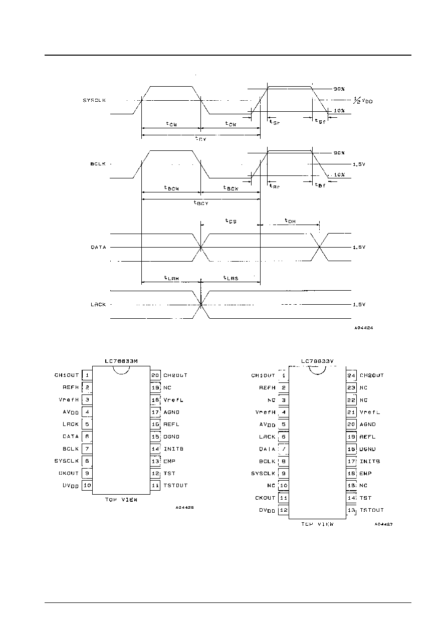
Audio Input Waveforms
Pin Assignments
No. 5212-4/11
LC78833M, 78833V
Pin Functions
No. 5212-5/11
LC78833M, 78833V
Pin No.
Pin
Description
LC78833M
LC78833V
1
1
CH1OUT
Channel 1 analog output
2
2
REFH
High-level reference voltage
Normally connected to AGND through a capacitor.
--
3
NC
No connection
3
4
Vref H
High-level reference voltage input
4
5
AV
DD
Analog system power supply
5
6
LRCK
LR clock input
A high level specifies channel 1 and a low level channel 2.
6
7
DATA
Digital audio data input
Accepts data in a two's complement MSB first format.
7
8
BCLK
Bit clock input
8
9
SYSCLK
System clock input (384fs)
--
10
NC
No connection
9
11
CKOUT
System clock output (384fs)
10
12
DV
DD
Digital system power supply
11
13
TSTOUT
Test output
12
14
TST
Test output
This pin must be connected to DGND in normal operation.
--
15
NC
No connection
De-emphasis filter on/off control input
13
16
EMP
A high level specifies on and a low level off.
This function supports a sampling frequency fs of 44.1 kHz.
14
17
INITB
Initialization input. A low level input to this pin initializes the IC.
15
18
DGND
Digital system ground
16
19
REFL
Low-level reference voltage
Normally connected to AGND through a capacitor.
17
20
AGND
Analog system power supply
18
21
Vref L
Low-level reference voltage input
--
22
NC
No connection
19
23
NC
No connection
20
24
CH2OUT
Channel 2 analog output