 | –≠–ª–µ–∫—Ç—Ä–æ–Ω–Ω—ã–π –∫–æ–º–ø–æ–Ω–µ–Ω—Ç: LC78857V | –°–∫–∞—á–∞—Ç—å:  PDF PDF  ZIP ZIP |

Overview
The LC78857V is a sigma-delta type D/A converter for
use in digital audio systems. It provides both digital and
analog filters on chip.
Features
∑ Built-in 8x oversampling digital filters: 3-stage FIR
structure (31st order, 11th order, and 3rd order filters)
∑ Analog low-pass filter
∑ Digital deemphasis (handles Fs = 44.1 kHz operation)
∑ Digital attenuator
∑ Soft muting
∑ Supports a 384fs system clock rate.
∑ 5-V single-voltage power supply
∑ Fabricated in a silicon gate CMOS process.
Package Dimensions
unit: mm
3175A-SSOP24
CMOS IC
D3097HA (OT) No. 5537-1/11
Preliminaly
SANYO: SSOP24
[LC78857V]
SANYO Electric Co.,Ltd. Semiconductor Bussiness Headquarters
TOKYO OFFICE Tokyo Bldg., 1-10, 1 Chome, Ueno, Taito-ku, TOKYO, 110-0005 JAPAN
Digital Audio D/A Converter IC
with On-Chip Digital Filters
LC78857V
Ordering number : EN
*
5537A
Parameter
Symbol
Conditions
Ratings
Unit
Maximum supply voltage
V
DD
max
≠0.3 to +7.0
V
Input voltage
V
IN
≠0.3 to V
DD
+0.3
V
Output voltage
V
OUT
≠0.3 to V
DD
+0.3
V
Operating temperature
Topr
≠30 to +75
∞C
Storage temperature
Tstg
≠40 to +125
∞C
Specifications
Absolute Maximum Ratings
at V
SS
= 0 V
Parameter
Symbol
Conditions
Ratings
Unit
min
typ
max
Supply voltage
V
DD
3.5
5.0
5.5
V
Input voltage
T
IN
0
V
DD
V
Operating temperature
Topr
≠30
+75
∞C
Allowable Operating Ranges
at Ta = 25∞C
No. 5537-2/11
LC78857V
Parameter
Symbol
Conditions
Ratings
Unit
min
typ
max
Input high-level voltage (1)
V
IH
1
Pin 15
0.7 V
DD
V
Input low-level voltage (1)
V
IL
1
Pin 15
0.3 V
DD
V
Input high-level voltage (2)
V
IH
2
Pins 6, 7, 8, 9, 10, 11, 14, 18, and 19
2.2
V
Input low-level voltage (2)
V
IL
2
Pins 6, 7, 8, 9, 10, 11, 14, 18, and 19
0.8
V
Output high-level voltage
V
OH
I
OH
= ≠3 mA, pin 17
2.4
V
Output low-level voltage
V
OL
I
OL
= 3 mA, pin 17
0.4
V
Input leakage current
I
L
V
I
= V
SS
, V
DD
:
≠25
25
µA
Pins 6, 7, 8, 9, 10, 11, 14, 15, 18, and 19
Allowable power dissipation
Pd
V
DD
= 5.0 V
135
200
mW
DC Characteristics
at Ta = ≠30 to 75∞C, V
DD
= 3.5 to 5.5 V, V
SS
= 0 V
Parameter
Symbol
Conditions
Ratings
Unit
min
typ
max
Oscillator frequency
f
X
169
18.5
MHz
BCLK frequency
f
BCX
3.0
MHz
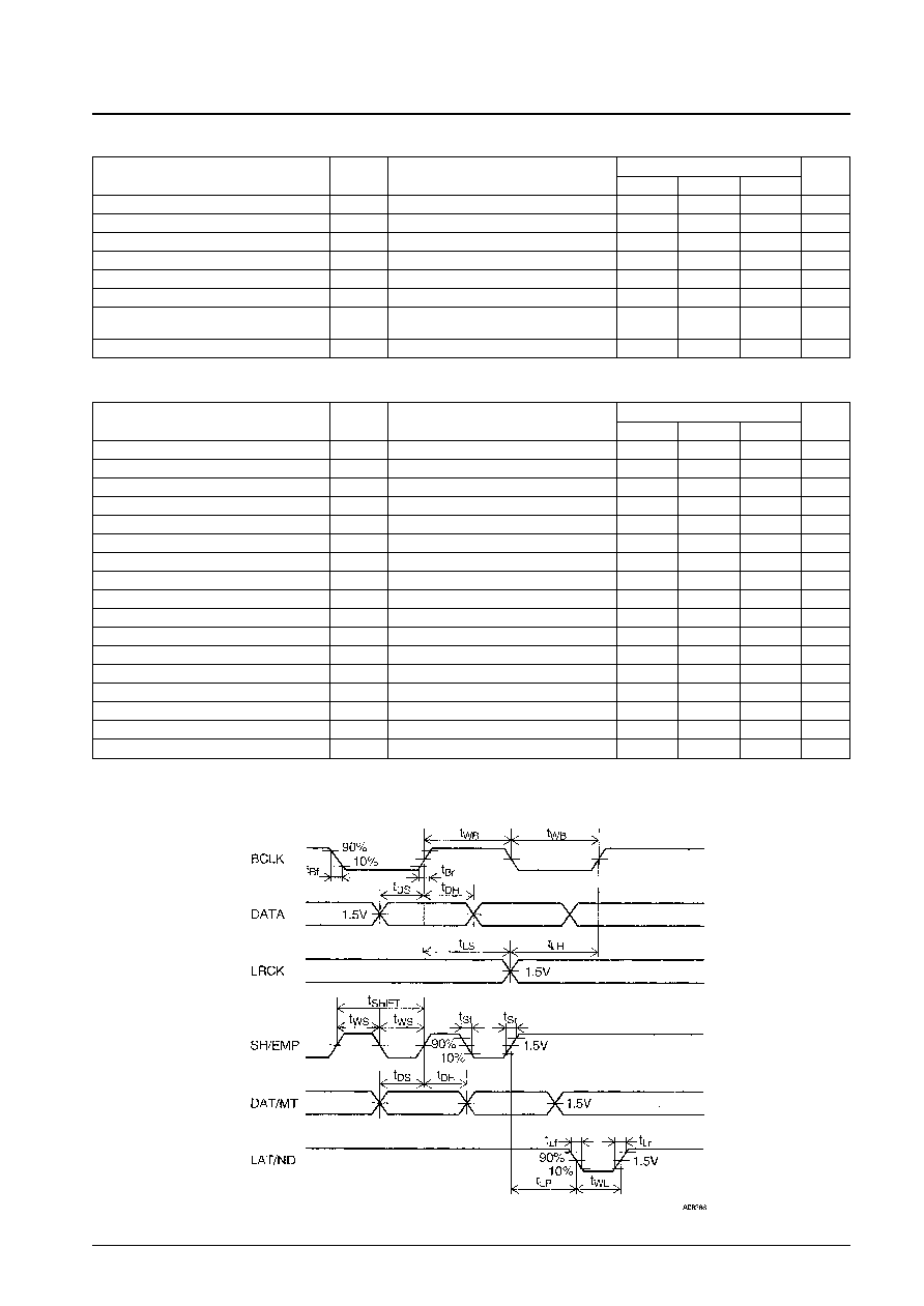
BCLK pulse width
t
WB
100
ns
BCLK rise time
t
Br
30
ns
BCLK fall time
t
Bf
30
ns
DATA setup time
t
DS
20
ns
DATA hold time
t
DH
20
ns
LRCK setup time
t
LS
50
ns
LRCK hold time
t
LH
50
ns
SH/EMP pulse period
t
SHIFT
1000
ns
SH/EMP pulse width
t
WS
300
ns
SH/EMP rise time
t
Sr
100
ns
SH/EMP fall time
t
Sf
100
ns
LAT/ND pulse width
t
WL
300
ns
Latch pulse input time
t
LP
300
ns
LAT/ND rise time
t
Lr
100
ns
LAT/ND fall time
t
Lf
100
ns
AC Characteristics
at Ta = ≠30 to 75∞C, V
DD
= 3.5 to 5.5 V, V
SS
= 0 V
Timing Chart
No. 5537-3/11
LC78857V
Parameter
Symbol
Conditions
Ratings
Unit
min
typ
max
Total harmonic distortion
THD+N
1kHz, 0 dB
0.008
0.012
%
Signal-to-noise ratio
S/N
JIS-A
90
96
dB
Crosstalk
CT
1kHz, 0 dB
88
92
dB
Full scale output level
VFS
1 kHz, 0dB
2.8
3.0
3.2
Vp-p
Dynamic range
DR
JIS-A
84
87
dB
Output load resistance
R
L
Pins 2 and 23
5
k
Analog Characteristics
at Ta = 25∞C, V
DD
= 5.0 V
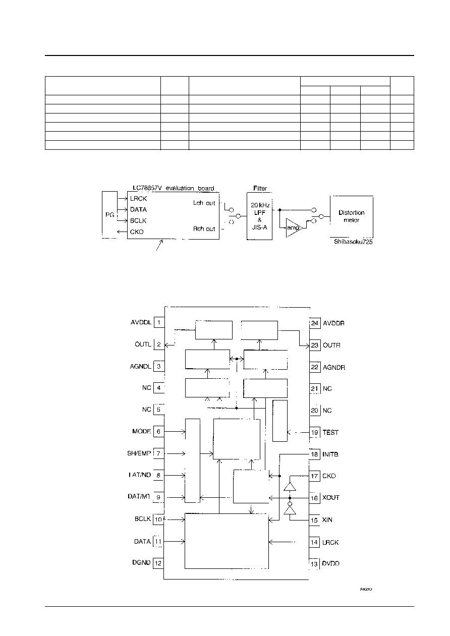
Test Circuit
PG: Pattern generator (signal generator)
Filter: Band limiting filter
Block Diagram
See the application circuit example
Analog low-
pass filter
(left channel)
Analog low-
pass filter
(right channel)
PWM output
circuit
(left channel)
PWM output
circuit
(right channel)
Noise shaper
(left channel)
Noise shaper
(right channel)
8
◊
oversampling
digital filters
Timing
generator
Interface circuit
Mode control circuit
Test circuit
No. 5537-4/11
LC78857V
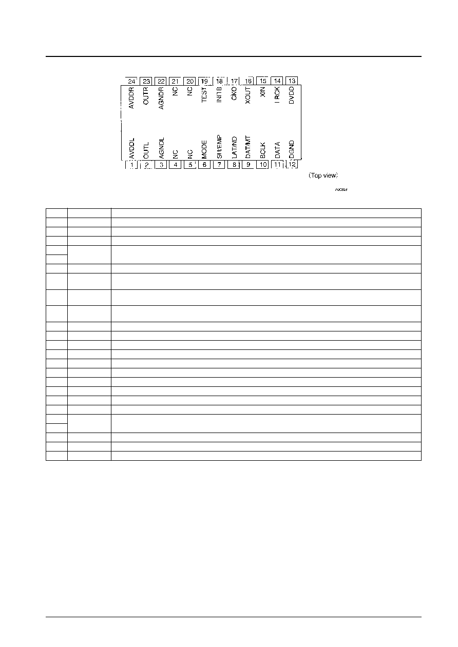
Pin Assignment
Pin Functions
Pin No.
Symbol
Function
1
AVDDL
Analog system power supply (left channel)
2
OUTL
Analog output (left channel)
3
AGNDL
Analog system ground (left channel)
4
NC
No Connection
5
6
MODE
Serial/parallel input mode selection
7
SH/EMP
When MODE is low: Control data shift signal (serial mode)
When MODE is high: Emphasis on/off switching (parallel mode)
8
LAT/ND
When MODE is low: Control data latch signal (serial mode)
When MODE is high: normal speed/double speed switching (parallel mode)
9
DAT/MT
When MODE is low: Control data input (serial mode)
When MODE is high: Soft muting control input (parallel mode)
10
BCLK
Bit clock input
11
DATA
Digital audio data input
12
DGND
Digital system ground
13
DV
DD
Digital system power supply
14
LRCK
LR clock input
15
XIN
Crystal oscillator element input
16
XOUT
Crystal oscillator element output
17
CKO
Clock output (384fs)
18
INITB
Initialization signal input (The IC internal state is initialized on a low input.)
19
TEST
Test pin (This pin must be connected to DGND during normal operation.)
20
NC
No Connection
21
22
AGNDR
Analog system ground (right channel)
23
OUTR
Analog output (right channel)
24
AVDDR
Analog system power supply (right channel)
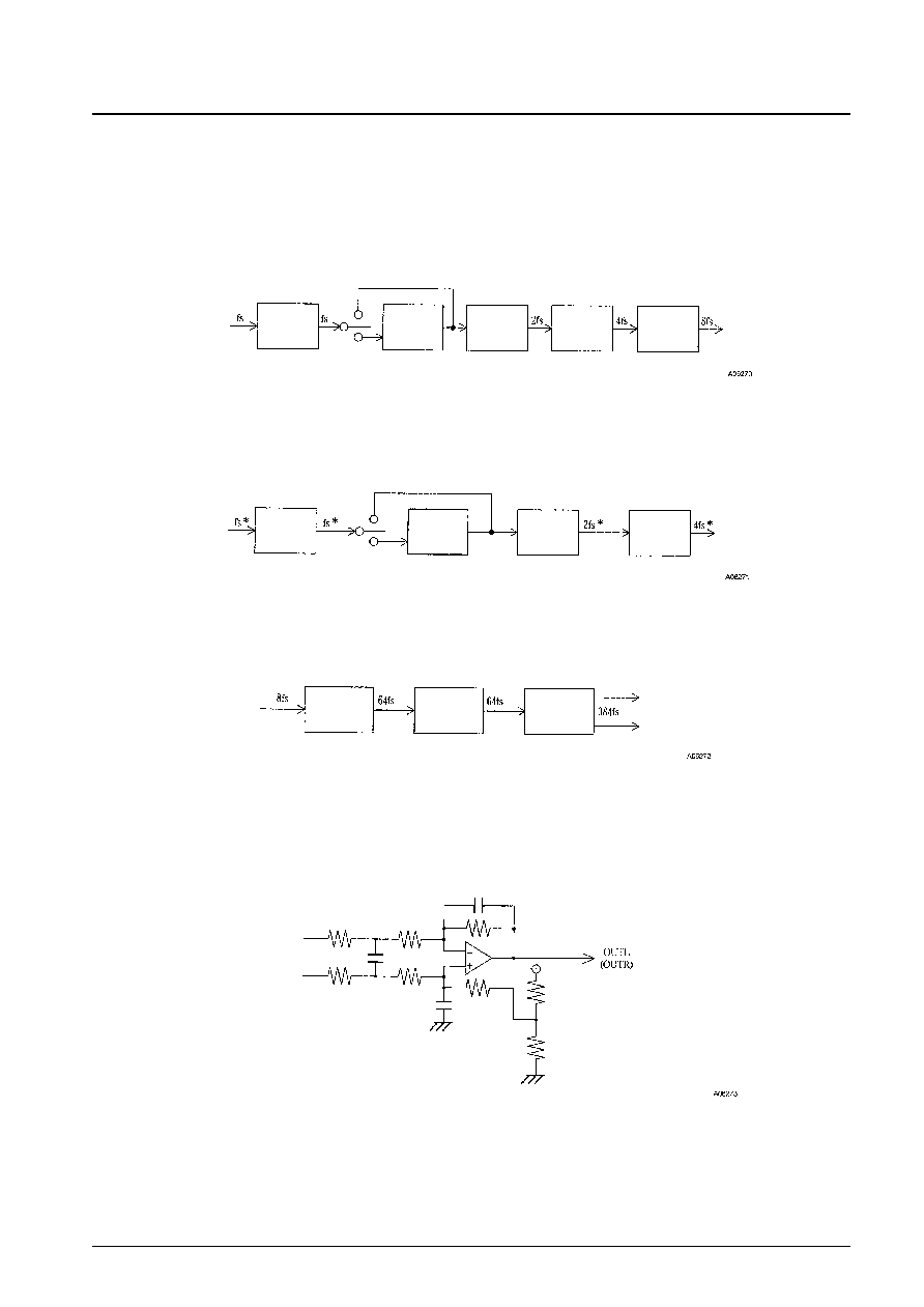
Circuit Operation
The LC78857V consists of three main blocks: the digital filter block, the sigma-delta D/A converter block, and the
analog filter block.
[Digital Filter Block]
The LC78857V performs the following calculations.
∑ Normal speed mode:
∑ Double speed mode:
This mode is used, for example, when dubbing a CD to cassette tape at double speed. Although the XIN has the same
frequency as normal speed mode, BCLK, LRCK, and DATA are input at twice the rate used in normal speed.
[Sigma-Delta D/A Converter Block]
This circuit accepts 8fs data input and outputs a 384fs 1-bit data sequence.
[Analog Low-Pass Filter Block]
This block consists of an analog low-pass filter that consists of on-chip resistors, capacitors, and operational amplifiers.
This block converts the 384fs 1-bit data streams A and B directly to an analog voltage output.
No. 5537-5/11
LC78857V
Input
Attenuator
Deemphas
is first-
order IIR
filter
31st-order
FIR filter
11th-order
FIR filter
3rd-order
FIR filter
To the sigma-delta
D/A converter
Input
Attenuator
Deemphas
is first-
order IIR
filter
31st-order
FIR filter
3rd-order
FIR filter
To the sigma-delta
D/A converter
fs
*
= double speed input = 2
◊
fs.
From the
digital filters
Front-end
interpolation
3rd-order
noise
shaper
PWM D/A
converter
1-bit output A
1-bit output B
1-bit output A
1-bit output B