 | –≠–ª–µ–∫—Ç—Ä–æ–Ω–Ω—ã–π –∫–æ–º–ø–æ–Ω–µ–Ω—Ç: LC78858V | –°–∫–∞—á–∞—Ç—å:  PDF PDF  ZIP ZIP |

SANYO Electric Co.,Ltd. Semiconductor Bussiness Headquarters
TOKYO OFFICE Tokyo Bldg., 1-10, 1 Chome, Ueno, Taito-ku, TOKYO, 110-8534 JAPAN
Overview
The LC78858V is a sigma-delta type D/A converter for
use in digital audio systems. It provides both digital and
analog filters on chip.
Features
∑ Built-in 8
◊
oversampling digital filters: 3-stage FIR
structure (31st order, 11th order, and 3rd order filters)
∑ Built-in third-order analog low-pass filter
∑ Digital deemphasis (handles Fs = 44.1 kHz operation)
∑ Digital attenuator (128 steps)
∑ Soft muting
∑ Digital bass boost
∑ Supports 256 fs and 384 fs system clocks
∑ 2.4 to 3.3V single-voltage power supply
∑ Fabricated in a silicon gate CMOS process.
Package Dimensions
unit: mm
3175A-SSOP24
CMOS IC
102098RM (OT) No. 5967-1/12
Preliminaly
SANYO: SSOP24
[LC78858V]
Digital Audio D/A Converter IC
with On-Chip Digital Filters
LC78858V
Ordering number : EN
*
5967
Parameter
Symbol
Conditions
Ratings
Unit
Maximum supply voltage
V
DD
max
≠0.3 to +4.6
V
Input voltage
V
IN
≠0.3 to V
DD
+0.3
V
Output voltage
V
OUT
≠0.3 to V
DD
+0.3
V
Operating temperature
Topr
≠30 to +75
∞C
Storage temperature
Tstg
≠40 to +125
∞C
Specifications
Absolute Maximum Ratings
at V
SS
= 0 V
Parameter
Symbol
Conditions
Ratings
Unit
min
typ
max
Supply voltage
V
DD
2.4
3.0
3.6
V
Input voltage
T
IN
0
V
DD
V
Operating temperature
Topr
≠30
+75
∞C
Allowable Operating Ranges
at Ta = 25∞C
Any and all SANYO products described or contained herein do not have specifications that can handle
applications that require extremely high levels of reliability, such as life-support systems, aircraft's
control systems, or other applications whose failure can be reasonably expected to result in serious
physical and/or material damage. Consult with your SANYO representative nearest you before using
any SANYO products described or contained herein in such applications.
SANYO assumes no responsibility for equipment failures that result from using products at values that
exceed, even momentarily, rated values (such as maximum ratings, operating condition ranges, or other
parameters) listed in products specifications of any and all SANYO products described or contained
herein.

No. 5967-2/12
LC78858V
Parameter
Symbol
Conditions
Ratings
Unit
min
typ
max
Input high-level voltage
V
IH
Pins 6, 7, 8, 9, 10, 11, 14, 15, 18, 19, and 20
0.7 V
DD
V
Input low-level voltage
V
IL
Pins 6, 7, 8, 9, 10, 11, 14, 15, 18, 19, and 20
0.3 V
DD
V
Output high-level voltage
V
OH
I
OH
= ≠3 mA, pins 5 and 17
V
DD
≠ 0.8
V
Output low-level voltage
V
OL
I
OL
= 3 mA, pins 5 and 17
0.4
V
Input leakage current
I
L
V
I
= V
SS
, V
DD
:
≠15
+15
µA
Pins 6, 7, 8, 9, 10, 11, 14, 15, 18, 19, and 20
Allowable power dissipation
Pd
V
DD
= 3.0 V
40
55
mW
DC Characteristics
at Ta = ≠30 to +75∞C, V
DD
= 2.4 to 3.6 V, V
SS
= 0 V
Parameter
Symbol
Conditions
Ratings
Unit
min
typ
max
Oscillator frequency
f
X
16.9
18.5
MHz
BCLK frequency
f
BCX
3.0
MHz
BCLK pulse width
t
WB
100
ns
BCLK rise time
t
Br
30
ns
BCLK fall time
t
Bf
30
ns
DATA setup time
t
DS
20
ns
DATA hold time
t
DH
20
ns
LRCK setup time
t
LS
50
ns
LRCK hold time
t
LH
50
ns
SH/EMP pulse period
t
SHIFT
1000
ns
SH/EMP pulse width
t
WS
300
ns
SH/EMP rise time
t
Sr
100
ns
SH/EMP fall time
t
Sf
100
ns
LAT/DB1 pulse width
t
WL
300
ns
Latch pulse input time
t
LP
300
ns
LAT/DB1 rise time
t
Lr
100
ns
LAT/DB1 fall time
t
Lf
100
ns
AC Characteristics
at Ta = ≠30 to +75∞C, V
DD
= 2.4 to 3.6 V, V
SS
= 0 V
Timing Chart

No. 5967-3/12
LC78858V
Parameter
Symbol
Conditions
Ratings
Unit
min
typ
max
Total harmonic distortion
THD+N
1kHz, 0dB
0.008
0.01
%
Signal-to-noise ratio
S/N
JIS-A
90
96
dB
Crosstalk
CT
1kHz, 0dB
85
88
dB
Full scale output level
VFS
1kHz, 0dB
1.8
Vp-p
Dynamic range
DR
JIS-A
82
85
dB
Output load resistance
R
L
Pins 2 and 23
10
k
Analog Characteristics
at Ta = 25∞C, V
DD
= 3.0 V
Test Circuit
PG: Pattern generator (signal generator)
Filter: Band limiting filter
Block Diagram
See the sample application circuit
Analog low-
pass filter
(left channel)
Analog low-
pass filter
(right channel)
PWM output
circuit
(left channel)
PWM output
circuit
(right channel)
Noise shaper
(left channel)
Noise shaper
(right channel)
8
◊
oversampling
digital filters
Timing
generator
Interface circuit
Mode control circuit
Test circuit
No. 5967-4/12
LC78858V
Pin Functions
Pin No.
Symbol
Function
1
AVDDL
Analog system power supply (left channel)
2
OUTL
Analog output (left channel)
3
AGNDL
Analog system ground (left channel)
4
VRL
Left channel reference voltage output
5
ZDETC
L and R common zero data detection output
Outputs a high level when zero (0) data are input consecutively in both the left and right channels
6
MODE
Serial/parallel input mode selection
7
SH/EMP
When MODE is low: Control data shift (serial mode)
When MODE is high: Emphasis on/off switching (parallel mode)
8
LAT/DB1
When MODE is low: Control data latch (serial mode)
When MODE is high: Digital bass boost 1 setting (parallel mode)
9
DAT/DB2
When MODE is low: Control data input (serial mode)
When MODE is high: Digital bass boost 2 setting (parallel mode)
10
BCLK
Bit clock input
11
DATA
Digital audio data input
12
DGND
Digital system ground
13
DV
DD
Digital system power supply
14
LRCK
LR clock input
15
XIN
Crystal oscillator element input
16
XOUT
Crystal oscillator element output
17
CKO
Clock output (256 fs or 384 fs)
18
INITB
Initialization signal input (The IC internal state is initialized on a low input.)
19
TEST
Test pin (This pin must be connected to DGND during normal operation.)
20
MT
Soft muting input
21
VRR
Right channel reference voltage output
22
AGNDR
Analog system ground (right channel)
23
OUTR
Analog output (right channel)
24
AVDDR
Analog system power supply (right channel)
Circuit Operation
The LC78858V consists of three main blocks: the digital filter block, the sigma-delta D/A converter block, and the
analog filter block.
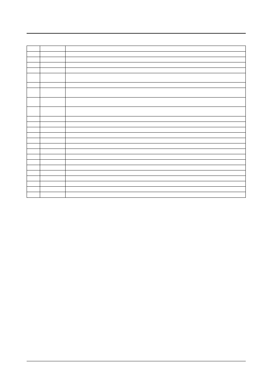
[Digital Filter Block]
The LC78858V performs the following calculations.
[Sigma-Delta D/A Converter Block]
This circuit accepts 8fs data input and outputs 256 fs or 384 fs 1-bit data sequence.
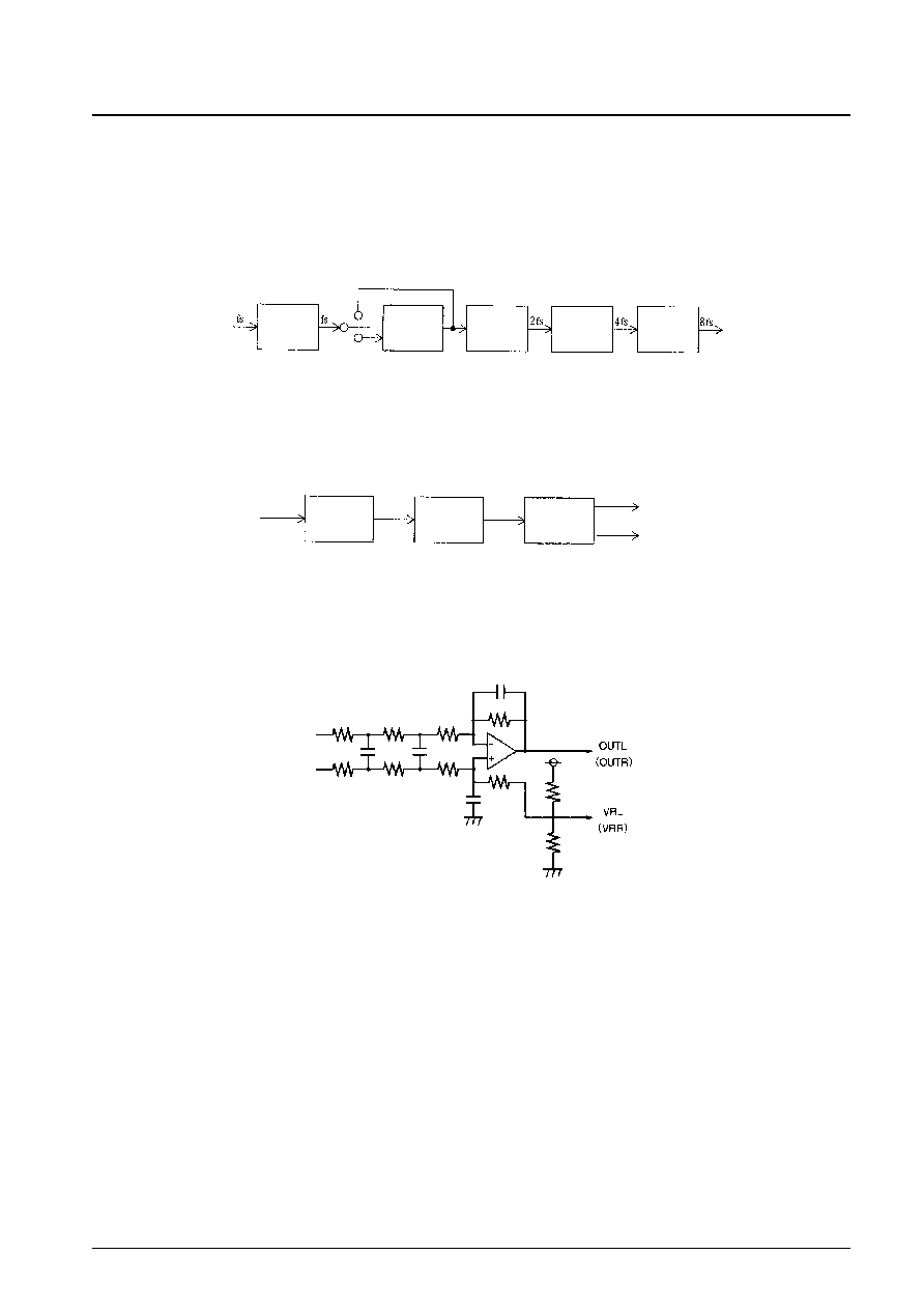
[Analog Low-Pass Filter Block]
This block consists of an analog low-pass filter that consists of on-chip resistors, capacitors, and operational amplifiers.
This block converts the 256 fs or 384 fs 1-bit data streams A and B directly to an analog voltage output.
No. 5967-5/12
LC78858V
Input
Attenuator
Deempha-
sis first-
order IIR
filter
31st-order
FIR filter
11th-order
FIR filter
3rd-order
FIR filter
To the sigma-delta
D/A converter
From the
digital filters
(8 fs)
(32 fs)
(32 fs)
8 fs
48 fs
48 fs
384 fs (256 fs)
Front-end
interpolation
3rd-order
noise
shaper
PWM D/A
converter
1-bit output A
1-bit output B
Items in parentheses
apply to 256 fs mode.
1-bit output A
1-bit output B