 | –≠–ª–µ–∫—Ç—Ä–æ–Ω–Ω—ã–π –∫–æ–º–ø–æ–Ω–µ–Ω—Ç: LC7942YD | –°–∫–∞—á–∞—Ç—å:  PDF PDF  ZIP ZIP |
LC7942YD
SANYO Electric Co., Ltd. Semiconductor Company
TOKYO OFFICE Tokyo Bldg., 1-10, 1 Chome, Ueno, Taito-ku, TOKYO, 110-8534 JAPAN
63099RM (ID) No. 6160--1/7
Ordering number: EN 6160
s
Any and all SANYO products described or contained herein do not have specifications that can handle
applications that require extremely high levels of reliability, such as life-support systems, aircraft's
control systems, or other applications whose failure can be reasonably expected to result in serious
physical and/or material damage. Consult with your SANYO representative nearest you before using
any SANYO products described or contained herein in such applications.
s
SANYO assumes no responsibility for equipment failures that result from using products at values that
exceed, even momentarily, rated values (such as maximum ratings, operating condition ranges, or other
parameters) listed in products specifications of any and all SANYO products described or contained
herein.
CMOS IC
Dot-matrix LCD Driver
Overview
The LC7942YD is a common driver IC for driving large,
dot
≠
matrix LCD displays. It features a built
≠
in 64
≠
bit
bidirectional shift register and a 4
≠
level LCD driver. It can
also be connected in cascade to increase the number of
bits.
The LC7942YD is designed to be used with LC7940YD
(QFP100) or LC7941YD (QFP100) segment drivers to
drive large LCD panels.
Features
∑ 64 built
≠
in LCD display drive circuits
∑ l/64 to 1/128 display duty cycle
∑ Input/outputs for cascade connection
∑ Bias supply voltages can be supplied externally
∑ Operating supply voltage and ambient temperature
- 2.7 to 5.5V logic supply (V
DD
) at Ta =
≠
20 to +85 ∞C
- 8 to 20 V LCD supply (V
DD
≠
V
EE
) at Ta =
≠
20 to
+85 ∞C
∑ CMOS process
∑ 80
≠
pin flat plastic package
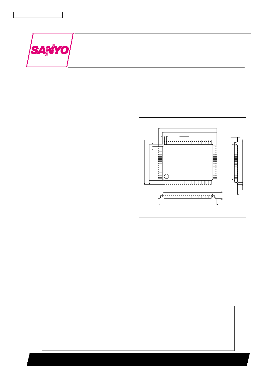
Package Dimensions
unit: mm
3177
≠
QFP80D
[LC7942YD]
0.15
1.6
14.0
17.2
0.8
1
24
25
40
41
64
65
80
21.6
0.8
2.45max
1.0
2.15
15.6
0.8
1.6
0.35
23.2
20.0
0.8
0.8
SANYO : QFP80D (QIP80D)
LC7942YD
No. 6160--2/7
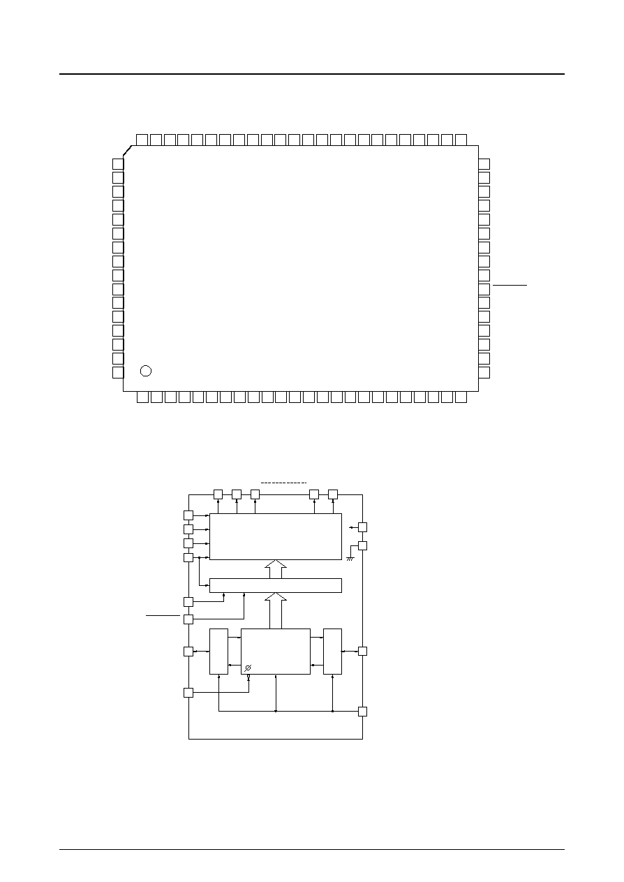
Pad Layout
(Top view)
Block Diagram
DI01
NC
CP
NC
M
NC
V
SS
RS/LS
V
DD
DISP OFF
V1
V2
V5
V
EE
NC
DI064
40
39
38
37
36
35
34
33
32
31
30
29
28
27
26
25
65
66
67
68
69
70
71
72
73
74
75
76
77
78
79
80
64 63 62 61 60 59 58 57 56 55 54 53 52 51 50 49 48 47 46 45 44 43 42 41
1
2
3
4
5
6
7
8
9
10 11 12 13 14 15 16 17 18 19 20 21 22 23 24
O25
O26
O27
O28
O29
O30
O31
O32
O33
O34
O35
O36
O37
O38
O39
O40
O24
O23
O22
O21
O20
O19
O18
O17
O16
O15
O14
O13
O12
O11
O10
O9
O8
O7
O6
O5
O4
O3
O2
O1
O41
O42
O43
O44
O45
O46
O47
O48
O49
O50
O51
O52
O53
O54
O55
O56
O57
O58
O59
O60
O61
O62
O63
O64
LC7942YD
4 Level LCD Drive Circuit
(64 bits)
Level Shifter (64 bits)
V1
01
02
03
063 064
V2
V5
M
DISP OFF
DIO1
CP
V
SS
DIO64
RS/LS
I/O
I/O
V
DD
V
EE
Bidirectional
Shift Register
(64 bits)
LC7942YD
No. 6160--3/7
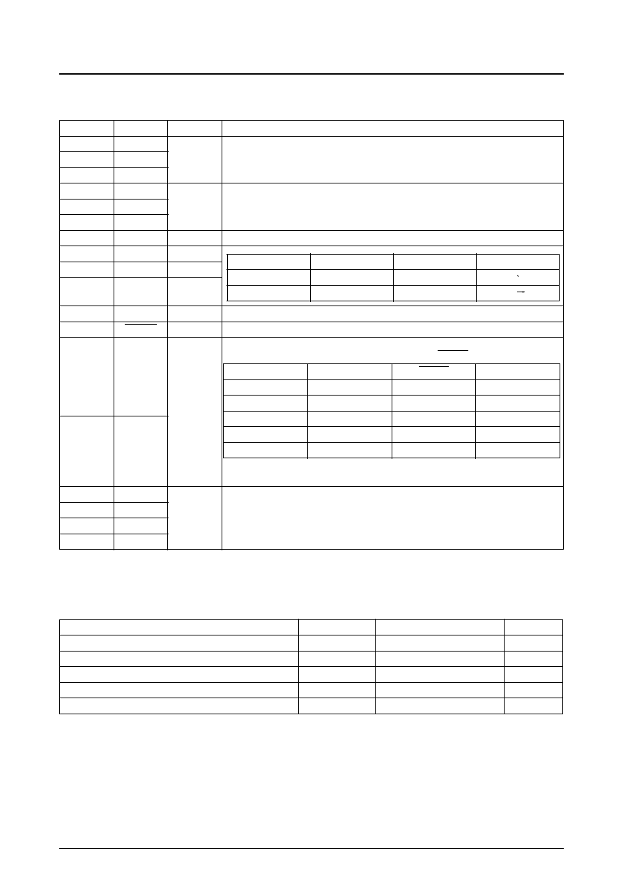
Pin Functions
Specifications
Absolute Maximum Ratings
at Ta = 25 ±2∞C, V
SS
= 0 V
Note
V
DD
V
1
> V
2
>V
5
> V
EE
Number
Name
I/O
Function
32
V
DD
Supply
V
DD
≠ Vss is the logic supply.
V
DD
≠ VEE is the LCD supply.
34
V
SS
27
V
EE
30
V
1
Supply
LCD panel drive voltage supplies.
V
1
and VEE are selected levels.
V
2
and V5 are not≠selected levels.
29
V
2
28
V
5
38
CP
I
Display data input clock (falling≠edge trigger).
40
DIO1
I/O
25
DIO64
I/O
33
RS/LS
I
36
M
I
LCD panel drive voltage output alternation control signal.
31
DISP OFF
I
O1 to O64 output control input pins.
41 to 80
O
LCD drive outputs
The output drive level is determined by the display data, M signal and DISPOFF input as show below.
Note
◊
= don't care (tied HIGH or LOW)
O1 to O40
1 to 24
O41 to O64
26
NC
≠
No connection.
35
NC
37
NC
39
NC
Parameter
Symbol
Ratings
Unit
Logic supply voltage
V
DD
max
≠0.3 to +7.0
V
LCD supply voltage. See note.
V
DD
≠ V
EE
max
0 to 22
V
Input voltage
V
I
max
≠0.3 to V
DD
+ 0.3
V
Operating temperature range
T
opr
≠20 to +85
∞C
Storage temperature range
T
stg
≠40 to +125
∞C
RS/LS
DIO1
DIO64 Shift
direction
LOW (rlght shift)
Input
Output
O1
O64
HIGH (left shift)
Output
Input
O64
O1
M
Q
DISPOFF
Output
LOW
LOW
HIGH
V
2
LOW
HIGH
HIGH
V
EE
HIGH
LOW
HIGH
V
5
HIGH
HIGH
HIGH
V
1
◊
◊
LOW
V
1
LC7942YD
No. 6160--4/7
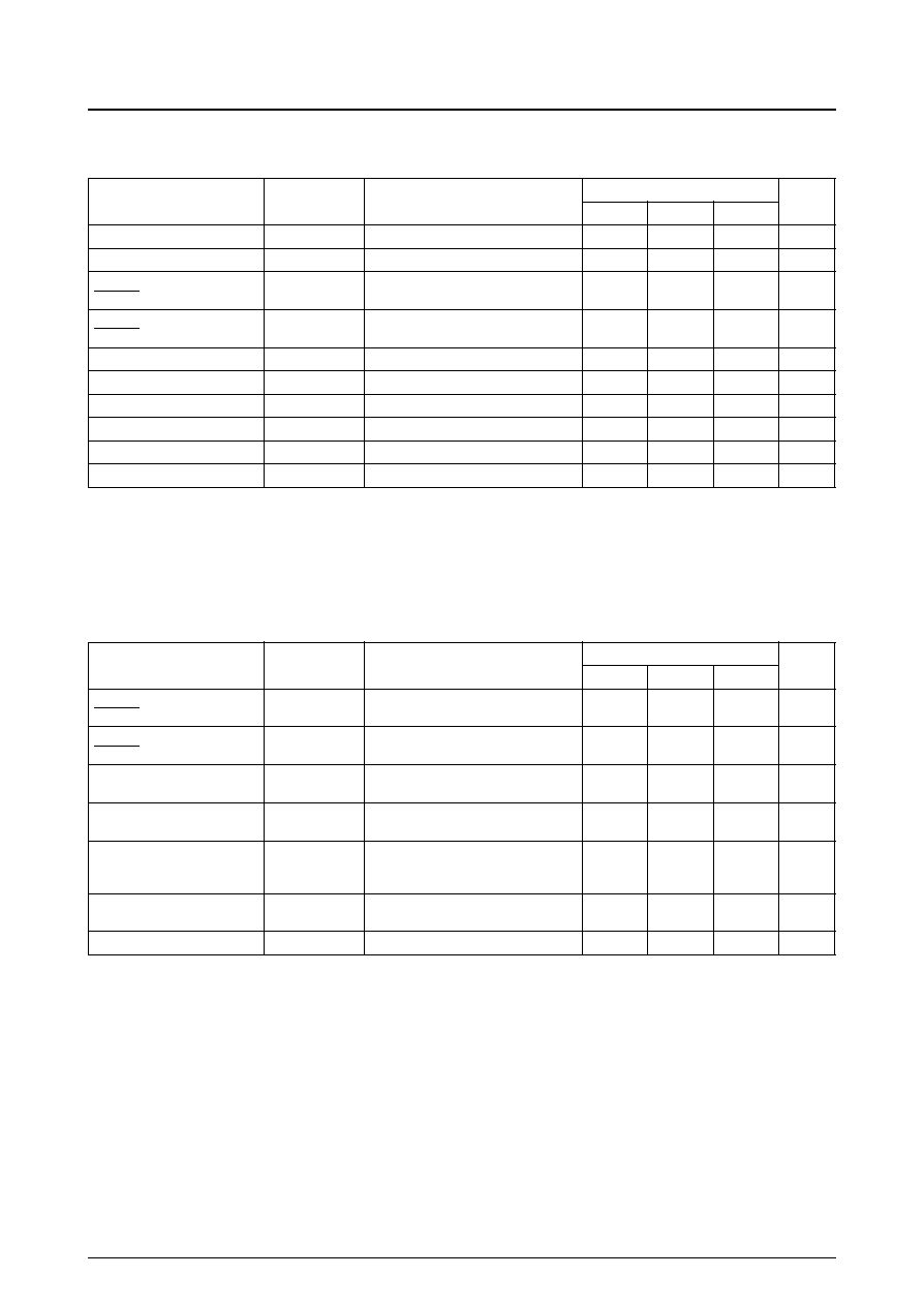
Allowable Operating Ranges
at Ta = ≠20 to +85 ∞C, V
SS
= 0 V
Note
1. V
DD
V
1
> V
2
> V
5
> V
EE
2. At turn ON, the LCD supply should be energized after or simultaneously with the logic supply. At turn OFF, the logic supply
should be cut after or simultaneously with the LCD supply.
Electrical Characteristics
at Ta = 25 ± 2 C, V
SS
= 0 V, V
DD
= 2.7 to 5.5 V
Note
V
DE
= V
1
or V
2
or V
5
or V
EE
, V
l
= V
EE
, V
2
= l0/11
◊
(V
DD
≠
V
EE
), V
5
= l/11
◊
(V
DD
≠
V
EE
)
Parameter
Symbol
Conditions
Ratings
Unit
min
typ
max
Logic supply voltage
V
DD
2.7
≠
5.5
V
LCD supply voltage
V
DD
≠ V
EE
See notes 1 and 2.
8
≠
20
V
DIO1, DIO64, CP, M, RS/LS and
DISPOFF HIGH≠level input voltage
V
IH
0.8V
DD
≠
≠
V
DIO1, DIO64, CP, M, RS/LS and
DISPOFF LOW≠level input voltage
V
IL
0.2V
DD
≠
≠
V
CP shift clock frequency
f
CP
≠
≠
1
MHz
CP pulsewidth
t
WC
125
≠
≠
ns
DIO1 and DIO64 to CP setup time
t
SETUP
l00
≠
≠
ns
DIOI and DIOS4 to CP hold time
t
HOLD
l00
≠
≠
ns
CP rise time
t
R
≠
≠
50
ns
CP fall time
t
F
≠
≠
50
ns
Parameter
Symbol
Conditions
Ratings
Unit
min
typ
max
DIO1, DIO64, CP, M, RS/LS and
DISPOFF HIGH≠level input current
I
IH
V
IN
= V
DD
≠
≠
1
µA
DIO1, DIO64, CP, M, RS/LS and
DISPOFF LOW≠level input current
I
IL
V
IN
= V
SS
≠
1
≠
≠
µA
DIO1 and DIO64 HIGH≠level output
voltage
V
OH
I
OH
= ≠400 µA
V
DD
≠ 0.4
≠
≠
V
DIO1 and DIO64 LOW≠level output
voltage
V
OL
I
OL
= 400 µA
≠
≠
0.4
V
O1 to O64 driver ON resistance
R
ON
V
DD
≠ V
EE
= 18 V,
V
DD
≠ V
OL
= 0.25 V,
V
DD
= 4.5 V
≠
≠
1.5
k
V
DD
static supply current
I
DD
V
DD
≠ V
EE
= 18 V,
CP = V
DD
≠
≠
100
µA
CP input capacitance
C
I
f
CP
= 1 MHz
≠
5
≠
pF
LC7942YD
No. 6160--5/7
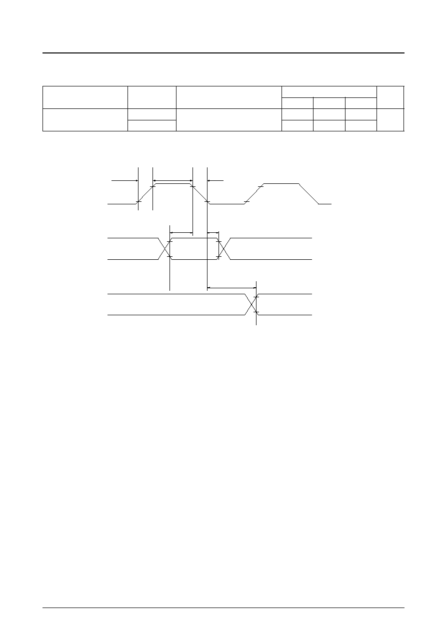
Switching Characteristics
at Ta = 25 ± 2 ∞C, V
SS
= 0 V, V
DD
= 2.7 to 5.5 V
Switching Characteristics Waveform
Parameter
Symbol
Conditions
Ratings
Unit
min
typ
max
Output delay time
t
PLH
C
L
≠
30 pF
≠
≠
250
ns
t
PHL
≠
≠
250
twc
tR
CP
DIO1
(DIO64)
DIO64
(DIO1)
tF
tSET
UP
tHOLD
0.8V
DD
0.2V
DD
tPLH,tPHL