 | –≠–ª–µ–∫—Ç—Ä–æ–Ω–Ω—ã–π –∫–æ–º–ø–æ–Ω–µ–Ω—Ç: LC7958NC | –°–∫–∞—á–∞—Ç—å:  PDF PDF  ZIP ZIP |

42800RM6585-1/11
Preliminary
Overview
LC7958NC is a 64-bit constant current LED driver IC
designed to directly drive LED head array.
The output terminals for LED drive are arranged in
2-row staggered position of 80-
µ
m pitch at one side. It
enables drive of LED Array of 300-dpi in one side
disposition, 600dpi in both sides disposition
Features and Functions
∑
Logic voltage (VDD): +5 V
±
10 %
∑
LED drive current (IOH): 5.0 mA (TYP)
∑
Clock frequency (fc): 10 MHz
∑
Output current control circuit built in
∑
Mode switching function by the SEL pin
∑
Chip size: 1.43 mm
◊
5.39 mm
∑
Number of pads: 86
∑
64-bit shift register circuit
∑
64-bit latch circuit
∑
Output driver on/off switching function
∑
Constant current circuit
∑
64-bit p-channel open drain LED driver
Any and all SANYO products described or contained herein do not have specifications that can handle
applications that require extremely high levels of reliability, such as life-support systems, aircraft's
control systems, or other applications whose failure can be reasonably expected to result in serious
physical and/or material damage. Consult with your SANYO representative nearest you before using
any SANYO products described or contained herein in such applications.
SANYO assumes no responsibility for equipment failures that result from using products at values that
exceed, even momentarily, rated values (such as maximum ratings, operating condition ranges, or other
parameters) listed in products specifications of any and all SANYO products described or contained
herein.
LC7958NC
64-Bit LED Driver for 300 dpi Printers
CMOS IC
Ordering number: ENN*6585
LC7958NC
6585-2/11
The characteristics shown below are those of devices encapsulated in the SANYO standard ceramic package
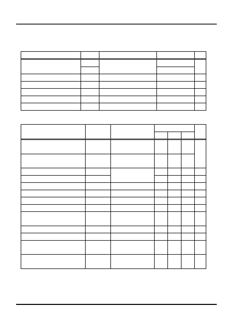
Specifications
Absolute Maximum Ratings
at Vss=0V
Parameter
Symbol
Conditions
Ratings
Unit
VDD1
-0.3 to 6.5
Power supply voltage
VDD2
Ta = 25
∞
C
-0.3 to 6.5
V
Input voltage
VI
Ta = 25
∞
C
-0.3 to VDD1+ 0.3
V
Output voltage
VO
Ta = 25
∞
C
-0.3 to VDD1+ 0.3
V
Driver output current
IOUT
0 to -10
m A
Operating Junction temperature
Tj
-10 to 125
∞
C
Storage temperature
Tstg
-35 to 125
∞
C
Allowable Operating Ranges
at Vss = 0 V, VDD1 = VDD2 = 5 V
±
10%, Ta = 0 to 100
∞
C
Ratings
Parameter
Symbol
Conditions
min
typ
max
Unit
Power supply voltage
VDD1,VDD2
VDD1(pad 2),
VDD2(pad 6)
4.5
5.5
Potential difference*1
VDF
Between VDD1 and
VDD2
-0.3
0
0.3
V
High-level input voltage
VIH
2.0
VDD1
V
Low-level input voltage
VIL
All inputs
0
0.8
V
Clock frequency
fc
CLOCK 1
10
MHz
Clock duty
D CLK
CLOCK 1
35
50
65
%
Setup time from SI to CLOCK1
tsc
SI, CLOCK 1
30
ns
Hold time from CLOCK1 to SI
thold
SI, CLOCK 1
10
ns
Setup time from CLOCK1 to
LOAD1
tSL
LOAD 1, CLOCK 1
50
ns
Hold time from LOAD1 to CLOCK1
tHL
LOAD 1, CLOCK 1
50
ns
LOAD1 pulse width
tWL
LOAD 1
40
ns
CLOCK1 rise/fall time
tCr
tCf
CLOCK 1
35
ns
LOAD1 rise/fall time
tLr
tLf
LOAD 1
35
ns
*1:In case potential difference occurred between VDD1 and VDD2, Driver current value changes. Therefore using it with
VDD1=VDD2 is recommended.
LC7958NC
6585-3/11
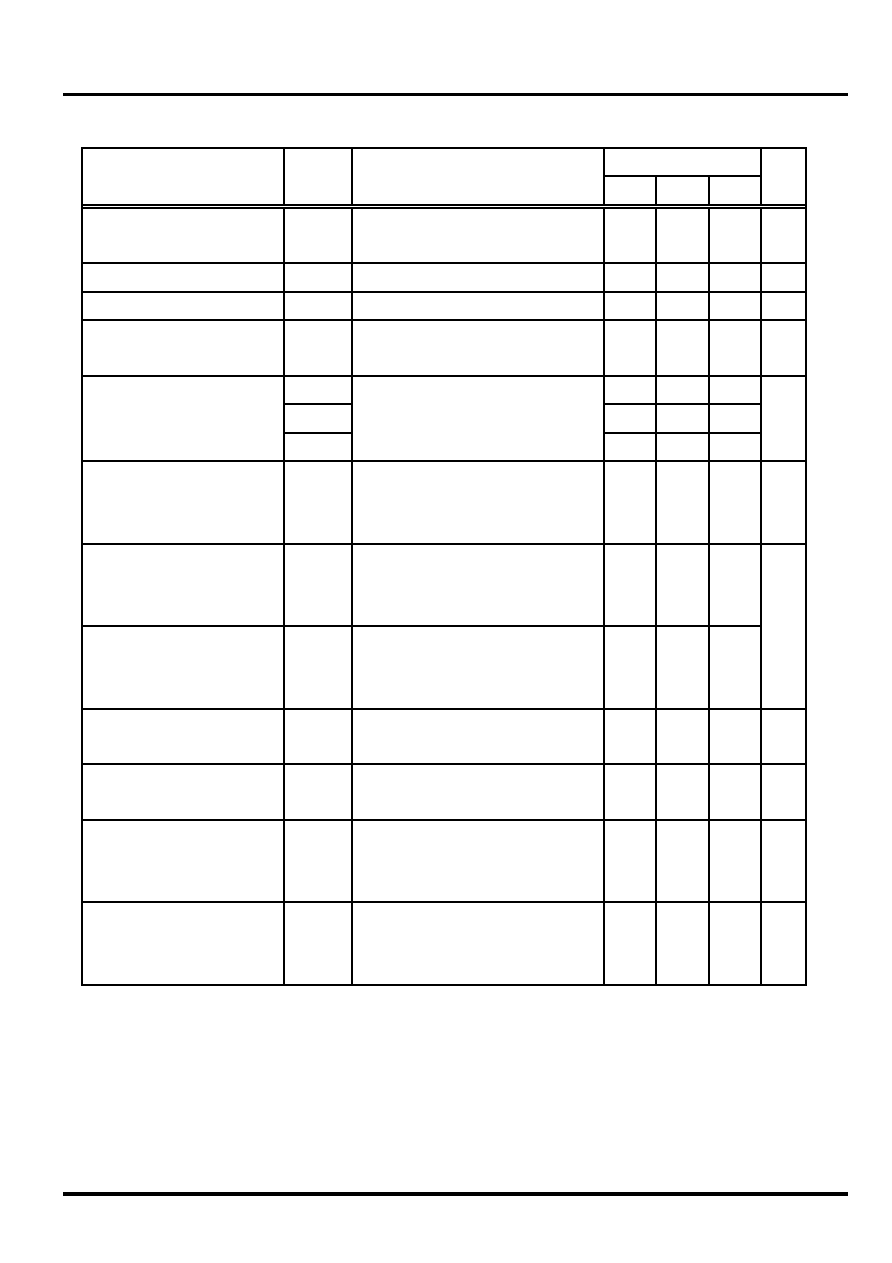
Electrical Characteristics
at VSS = 0 V, VDD1 = VDD2 = 5 V
±
10%, Ta = 0 to 100
∞
C
Ratings
Parameter
Symbol
Conditions
min
typ
max
Unit
High-level output voltage
VOH
LOAD2, S0, CLOCK2: IO = -200
µ
A
VDD -
0.5
V
Low-level output voltage
VOL
LOAD2, S0, CLOCK2: IO = 200
µ
A
0.5
V
Clock frequency
fc
10
MHz
High-level input current
IIH
All input pads: VDD1 = 5.5 V, VI =
5.5 V
1.0
µ
A
IIL1
-1.0
IIL2
-8
-25
-50
Low-level input current
IIL3
LOAD1, SI, CLOCK1, STROBE,
SEL, ADJ(-), ADJ(+): VDD1 = VDD2
= 5.5 V, VI = 0 V
-40
-100
-200
µ
A
High-level output current
IOH1
DO1 to DO64: operation mode 1,
VDD1 = VDD2 = 5.0 V, VO = 1.6 V,
VREF = 1.8 V
-3.7
-5.0
-6.7
m A
High-level output current
minus correction
IOH2
DO1 to DO64: operation mode 2
VDD1 = VDD2 = 5.0 V, VO = 1.6 V,
VREF = 1.8 V
-4.5
-6.0
-7.0
High-level output current
plus correction
IOH3
DO1 to DO64: operation mode 3
VDD1 = VDD2 = 5.0 V, VO = 1.6 V,
VREF = 1.8 V
+4.5
+6.0
+7.0
%
High-level output current
relative error between bits
IOH
DO1 to DO64: with all bits on
-5.0
+5.0
%
Output off leakage current
IOL
DO1 to DO64: operation VDD1 =
5.5 V, VO = 0 V
0
-50
µ
A
Operating current drain
(mode 1)
IDD
VDD1: VDD1 = VDD2 = 5.5 V,
VREF = 1.8 V, fc = 10 MHz, with
DO1 to DO64 off
9.0
13.0
m A
Standby current
IDDS
VDD1: VDD1 = VDD2 = 5.5 V, VREF
= 1.8 V, with fc stopped, with DO1
to DO64 off
2.5
4.0
m A
LC7958NC
6585-4/11
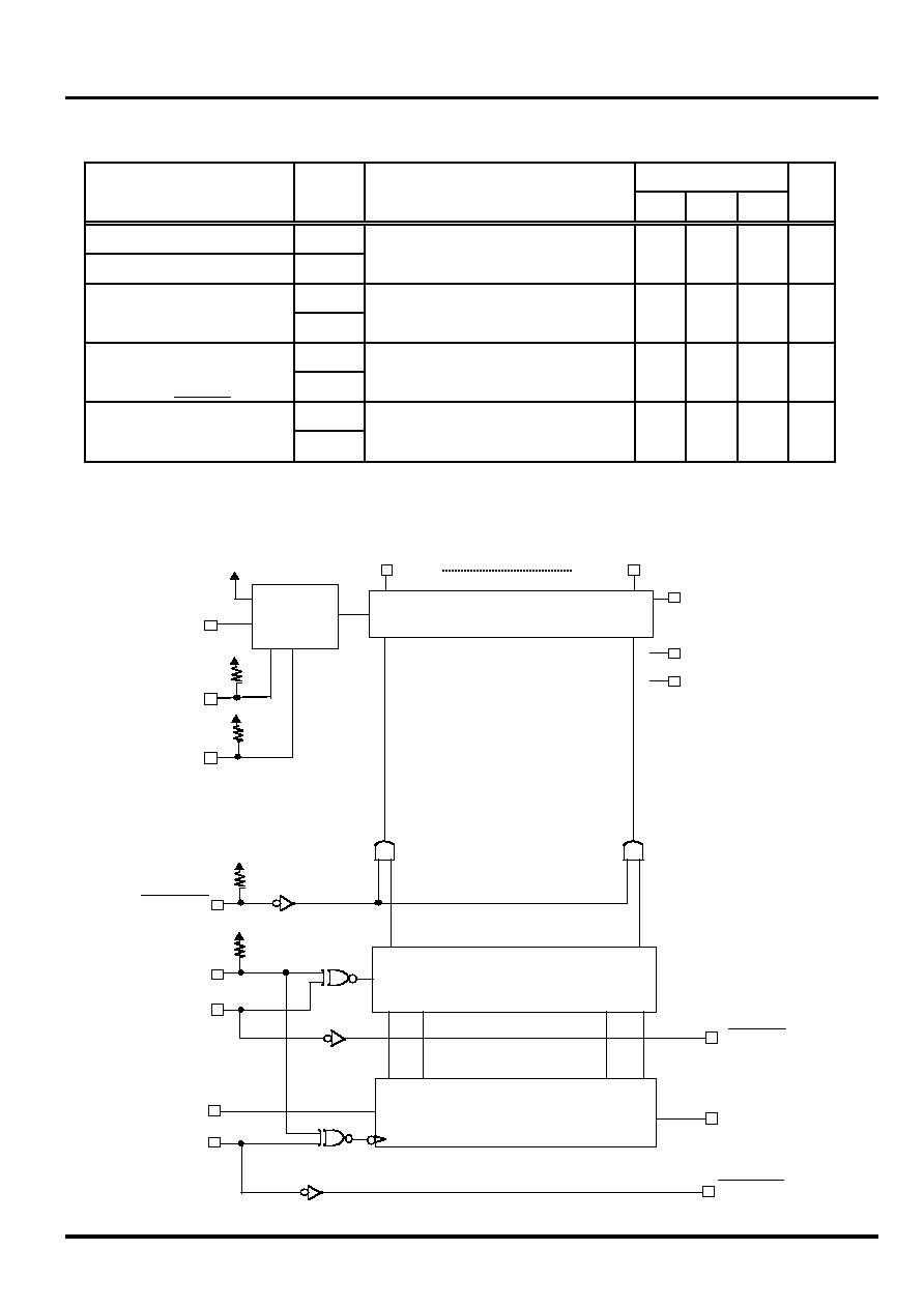
Switching Characteristics
at VSS = 0 V, VDD1 = VDD2 = 5 V
±
10%, Ta = 0 to 100
∞
C
Ratings
Parameter
Symbol
Conditions
min
typ
max
Unit
SO output rise time
tor
SO output fall time
tof
SO: CL=10.8pF
50
ns
tpsr
Output transmission delay
time from STROBE to DO
tpsf
STROBE, DO1 to DO64: CL = 10.8
pF, RF = 10 k
250
ns
tpcr
Output transmission delay
time from CLOCK2 to SO
tpcf
CLOCK2, SO
10
70
ns
tPH
CLOCK1
CLOCK2
transmission delay time
tPL
CLOC1, CLOCK2, LOAD1, LOAD2:
CL=10.8 pF
40
ns
Equivalent Circuit Block Diagram
CLOCK1
DO64
DO1
64-bit constant current driver
VREF
ADJ(+)
ADJ(-)
STROBE
VDD2
64-bit latch
64-bit shift register
SEL
LOAD1
SI
LOAD2
SO
CLOCK2
VDD1
VSS
Constant
current
circuit
LC7958NC
6585-5/11
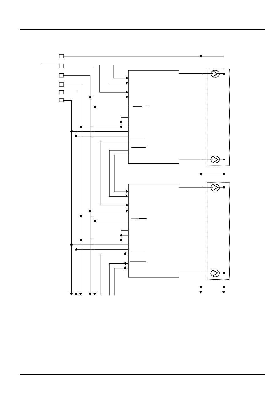
Sample Application Circuit Diagram
Note 1: The electric potential of the IC substrate is at VDD1.
Note 2: The number of cascade connection stages should be within 60. (10MHz)
Note 3: All VDD2 terminals should be bonded.
Note 4: Leave the SEL Terminal of the odd-numbered IC open, and connect the SEL terminal of even-numbered IC with
VSS.
Note 5: Apply the stable potential other than the VDD1 and VDD2 lines to the VREF terminal.
(To the next input stage)
OPEN
L
E
D
array
(Input signal)
LED
array
GND
STROBE
VREF
VSS
VDD1
VDD2
DO64
DO1
CL OCK1
SO
LOAD2
VSS
SEL
VDD 2
STROBE
LOAD1
SI
VREF
ADJ(-)
ADJ(+)
CL OCK
DO64
DO 1
CL OCK1
SO
LOAD
VSS
SEL
VDD 2
VDD 1
STROB
LOAD1
SI
VREF
ADJ(-)
ADJ(+)
CL OCK
VDD 1