 | –≠–ª–µ–∫—Ç—Ä–æ–Ω–Ω—ã–π –∫–æ–º–ø–æ–Ω–µ–Ω—Ç: LC7982A | –°–∫–∞—á–∞—Ç—å:  PDF PDF  ZIP ZIP |
Ordering number : EN5946
O1698RM (OT) No. 5946-1/18
Overview
The LC7982A is an LCD dot matrix graphics display
controller IC. It stores display data sent from an 8-bit
microcontroller in external display RAM and generates
dot matrix LCD drive signals. Applications can select
either of two modes: graphics mode, in which each bit in
external RAM controls the on/off state of an individual
pixel (dot) on the LCD, and character mode, in which
character codes are stored in external RAM and the dot
pattern is generated using the built-in character generator
ROM. Thus the LC7982A can support a wide range of
applications. The LC7982A is fabricated in a CMOS
process, and in conjunction with a CMOS microcontroller,
can implement low-power LCD display systems. This
device differs from the LC7981 only in the data stored in
the built-in character generator ROM.
Features
∑ LCD dot matrix and graphics display controller
∑ Display control capacity
Graphics mode
512 K dots (2
16
bytes)
Character mode
4096 characters (2
12
bytes)
∑ Character generator ROM 7360 bits
∑ European character support
Character font: 5
◊
7 dots
160 characters
Character font: 5
◊
11 dots 32 characters
(Can be expanded by up to 4 KB using external ROM.)
∑ Supports interfacing with 8-bit microcontrollers.
∑ Display duty (program selectable)
-- From static to 1/256 duty
∑ Extensive set of command functions
-- Scroll, cursor on/off/blink, character blinking, bit
manipulation
∑ Display methods : Method A and method B (program
selectable)
∑ Built-in oscillator circuit (Using an external resistor and
capacitor)
∑ Low power
∑ +5V single-voltage power supply
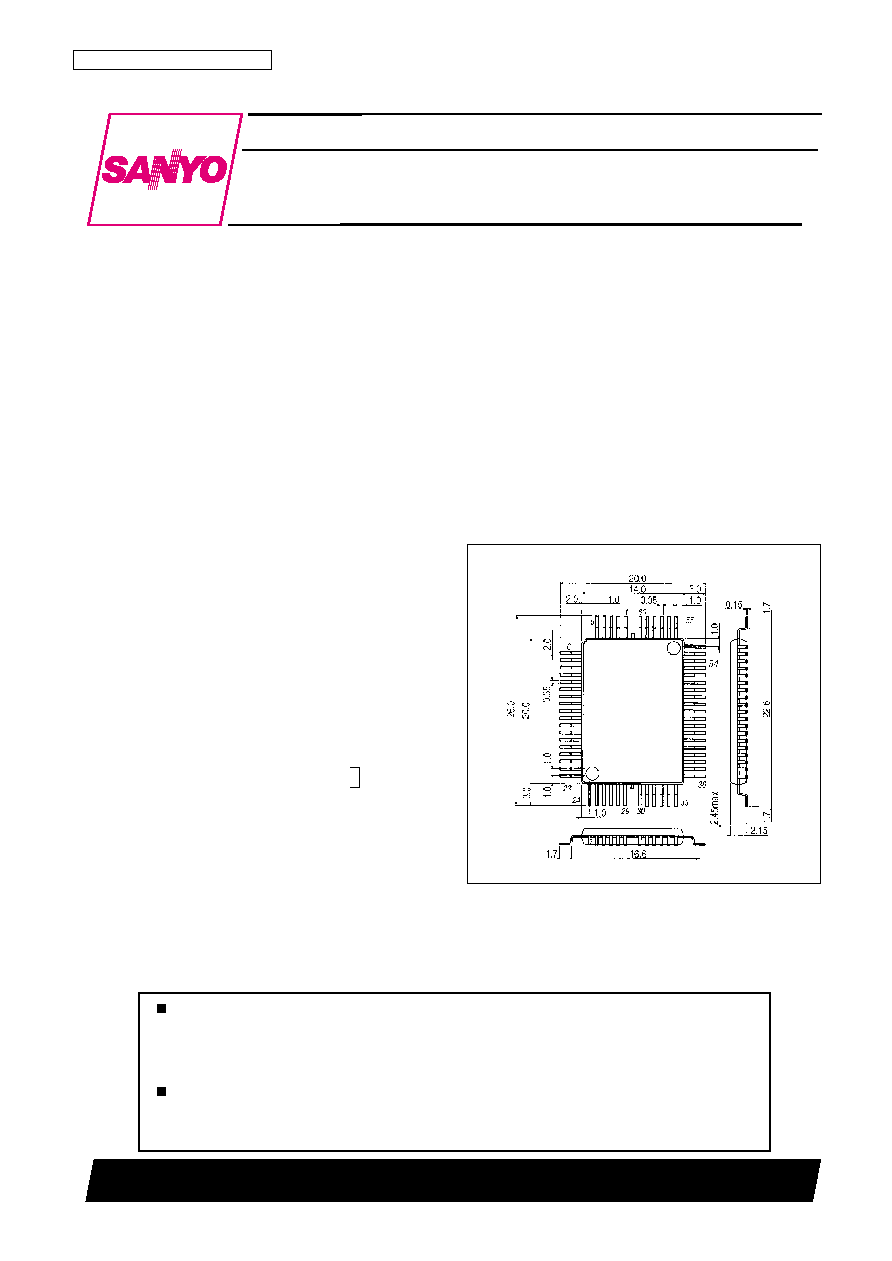
Package Dimensions
unit: mm
3055A-QFP60C
LC7982A
SANYO Electric Co.,Ltd. Semiconductor Bussiness Headquarters
TOKYO OFFICE Tokyo Bldg., 1-10, 1 Chome, Ueno, Taito-ku, TOKYO, 110-8534 JAPAN
LCD Dot Matrix Graphics Display Controller
CMOS IC
Any and all SANYO products described or contained herein do not have specifications that can handle
applications that require extremely high levels of reliability, such as life-support systems, aircraft's
control systems, or other applications whose failure can be reasonably expected to result in serious
physical and/or material damage. Consult with your SANYO representative nearest you before using
any SANYO products described or contained herein in such applications.
SANYO assumes no responsibility for equipment failures that result from using products at values that
exceed, even momentarily, rated values (such as maximum ratings, operating condition ranges, or other
parameters) listed in products specifications of any and all SANYO products described or contained
herein.
SANYO: QFP60C (QIP60C)
[LC7982A]
192 characters
total
Specifications
Absolute Maximum Ratings
at Ta = 25∞C, GND = 0 V
Allowable Operating Ranges
at Ta = ≠20 to +75∞C, GND = 0 V
Electrical Characteristics
at Ta = ≠20 to +75∞C, GND = 0 V, V
DD
= 5 V ±5%
No. 5946-2/18
LC7982A
Parameter
Symbol
Conditions
Ratings
Unit
Maximum supply voltage
V
DD
max
≠0.3 to +7.0
V
Input voltage
V
I
≠0.3 to V
DD
+0.3
V
Output voltage
V
O
≠0.3 to V
DD
+0.3
V
Allowable power dissipation
Pd max
Ta = 75∞C
200
mW
Operating temperature
Topr
≠20 to +75
∞C
Storage temperature
Tstg
≠55 to +125
∞C
Parameter
Symbol
Conditions
Ratings
Unit
min
typ
max
Supply voltage
V
DD
4.75
5.25
V
High-level input voltage
V
IH
1
Input and I/O pins other than SYNC and CR.
2.2
V
DD
V
Low-level input voltage
V
IL
1
Input and I/O pins other than SYNC and CR.
0
0.8
V
High-level input voltage
V
IH
2
SYNC, CR
0.7 V
DD
V
DD
V
Low-level input voltage
V
IL
2
SYNC, CR
0
0.3 V
DD
V
High-level output voltage
V
OH
1
I
OH
= ≠0.6 mA, DB0 to DB7, WE,
2.4
V
DD
V
MA0 to MA15, MD0 to MD7
Low-level output voltage
V
OL
1
I
OL
= 1.6 mA, DB0 to DB7, WE,
0
0.4
V
MA0 to MA15, MD0 to MD7
High-level output voltage
V
OH
2
I
OH
= ≠0.6 mA, SYNC, CPO, FLM,
V
DD
≠ 0.4
V
DD
V
CL1, CL2, D1, D2, MA, MB
Low-level output voltage
V
OL
2
I
OL
= 0.6 mA, SYNC, CPO, FLM,
0
0.4
V
CL1, CL2, D1, D2, MA, MB
[Internal Clock Operation]
Clock oscillator frequency
f
OSC
Cf = 15 pF ±5%, Rf = 39 k
±2%
*
1
500
600
700
kHz
[External Clock Operation]
Clock operating frequency
f
CP
*
2
2.5
MHz
Clock duty
Duty
*
3
47.5
50
52.5
%
Clock rise time
trcp
*
3
50
ns
Clock fall time
tfcp
*
3
50
ns
Parameter
Symbol
Conditions
Ratings
Unit
min
typ
max
Input leakage current
I
IN
V
IN
= 0 to V
DD
, CS, E, RS, R/W, RES
≠5
5
µA
Current drain
I
CC
1
RC oscillator, f
OSC
= 600 kHz
2
4
mA
I
CC
2
External clock, f
CP
= 2.5 MHz
3
5
mA
Pull-up current
I
PL
V
IN
= GND, DB0 to DB7, RD0 to RD7, MD0 to MD7
10
20
µA
(Note 1)
(Note 2)
(Note 3)
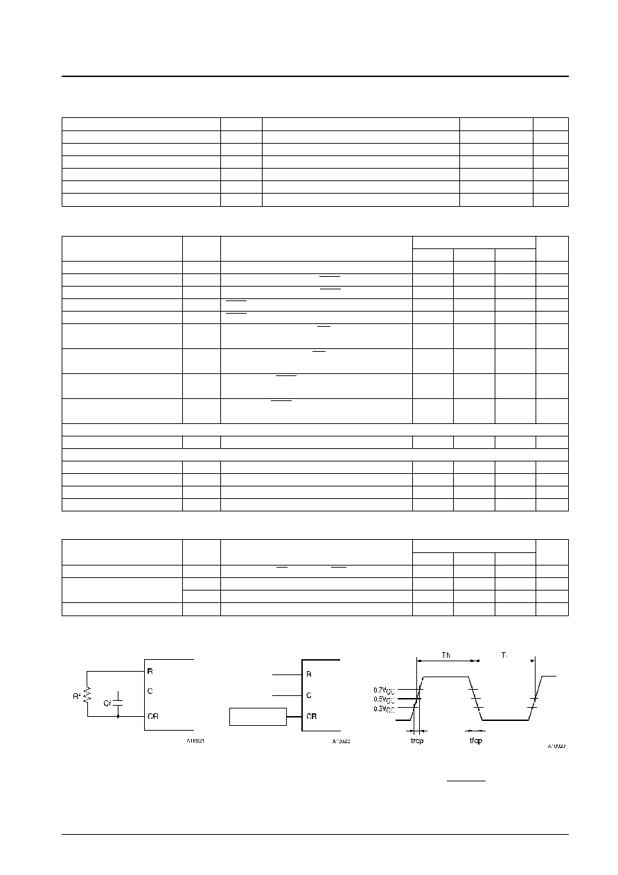
Cf = 15 pF ±5%
Rf = 39 k
±2%
(When f
OSC
= 600 kHz (typical))
Duty =
Th
◊
100%
Th + T1
Open
Open
Oscillator circuit
Timing Characteristics
∑ Bus read/write operation 1
Read cycle
Write cycle
Ta = ≠20 to +75∞C, V
DD
= 5V ±5%, GND = 0 V
Note: Test waveform definition
Input pins are driven to 2.4 V and 0.45 V, and the timing is measured at 1.5 V
No. 5946-3/18
LC7982A
DB0 to DB7
DB0 to DB7
Parameter
Symbol
Conditions
Ratings
Unit
min
typ
max
Address setup time
t
AS
90
ns
Address hold time
t
AH
10
ns
Data delay time (read)
t
DDR
C
L
= 50 pF
140
ns
Data hold time (read)
t
DHR
10
ns
Data setup time (write)
t
DSW
220
ns
Data hold time (write)
t
DHW
20
ns
Measurement point
∑ Bus read/write operation 2
Data read cycle
Data write cycle
Ta = ≠20 to +75∞C, V
DD
= 5V ±5%, GND = 0 V
Notes: ∑ For character display, HP is the number of dots in the horizontal direction per character,
and for graphics mode, HP is the number of bits shown on the display from each byte of display data.
∑ f
OSC
is the oscillator frequency, in units of MHz.
∑ All measurements are made at 1.5 V.
∑ Parallel operation (master mode)
Ta = ≠20 to +75∞C, V
DD
= 5V ±5%, GND = 0 V
Notes: ∑ With no loads on any of the output pins.
∑ Measurements are made at 0.5 V
DD
.
No. 5946-4/18
LC7982A
Parameter
Symbol
Instruction register value
Ratings
Unit
min
typ
max
Read cycle time
t
RCY
0DH
ns
Write cycle time
t
WCY
1
0EH, 0FH
ns
Write cycle time
t
WCY
2
0CH
ns
Write cycle time
t
WCY
3
00H, 01H, 02H, 03H, 04H,
ns
08H, 09H, 0AH, 0BH
(HP+2)
◊
10
3
+200
f
OSC
(2HP+2)
◊
10
3
+200
f
OSC
(HP+2)
◊
10
3
+200
f
OSC
2000
+200
f
OSC
Parameter
Symbol
Conditions
Ratings
Unit
min
typ
max
SYNC delay time
t
DSY
100
ns
SYNC pulse width
t
WSY
350
ns
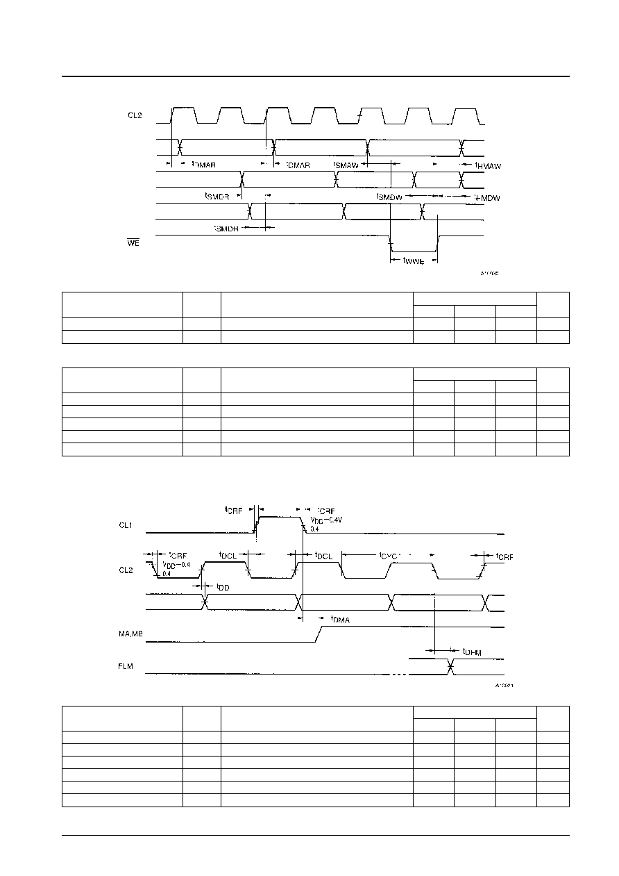
∑ External RAM and ROM interface
Read Cycle
at Ta = ≠20 to +75∞C, V
DD
= 5 V ±5%, GND = 0 V
Write Cycle
at Ta = ≠20 to +75∞C, V
DD
= 5 V ±5%, GND = 0 V
Notes: ∑ With no loads on any of the output pins.
∑ All measurements are made at 1.5 V.
∑ Driver IC interface
Ta = ≠20 to +75∞C, V
DD
= 5 V ±5%, GND = 0 V
Notes: ∑ With no loads on any of the output pins.
∑ Measurements other than those with a specified measurement point are made at 0.5 V
DD
.
No. 5946-5/18
LC7982A
Parameter
Symbol
Conditions
Ratings
Unit
min
typ
max
MA0 to MA15 read address delay time
t
DMAR
95
ns
MD0 to MD7, RD0 to RD7 setup time
t
SMDR
105
ns
Parameter
Symbol
Conditions
Ratings
Unit
min
typ
max
Memory address setup time
t
SMAW
50
ns
WE pulse width
t
WWE
350
ns
Memory data setup time
t
SMDW
250
ns
Memory address hold time
t
HMAW
50
ns
Memory data hold time
t
HMDW
50
ns
Parameter
Symbol
Conditions
Ratings
Unit
min
typ
max
Clock cycle time
t
CYC
400
ns
Clock phase difference
t
DCL
100
ns
Clock rise and fall times
t
CRF
30
ns
D1 and D2 phase difference
t
DD
100
ns
MA and MB phase difference
t
DMA
200
ns
FLM phase difference
t
DFM
200
ns
MA0 to
MA15
MD0 to
MD7
RD0 to
RD7
D1, D2