 | –≠–ª–µ–∫—Ç—Ä–æ–Ω–Ω—ã–π –∫–æ–º–ø–æ–Ω–µ–Ω—Ç: LC82101 | –°–∫–∞—á–∞—Ç—å:  PDF PDF  ZIP ZIP |
CMOS LSI
Ordering number : EN
*
4982A
63095HA (OT) No. 4982-1/5
Preliminary
SANYO Electric Co.,Ltd. Semiconductor Bussiness Headquarters
TOKYO OFFICE Tokyo Bldg., 1-10, 1 Chome, Ueno, Taito-ku, TOKYO, 110-8534 JAPAN
Image Processing Circuit
for FAX, Copier, and OCR Products
LC82101
Overview
The LC82101 converts an analog image signal from a
CCD or contact sensor to high-quality binary image data.
The LC82101 uses an internal 8-bit A/D converter for
A/D conversion, and in addition to the orthodox dithering
technique, also supports an error diffusion technique that
allows an even higher quality image to be acquired. These
techniques apply to the whole range of processing
supported by the LC82101, including full-pixel distortion
correction, gamma conversion for arbitrary gamma
curves, image compression processing, two-dimensional
filtering, halftone processing, and image separation
processing to separate documents into text, photograph,
and halftone regions. Thus this LSI implements the image
processing required by FAX, copier, and OCR systems.
Features
∑ Number of pixels processed
2048 pixels/line (64 KB memory, white correction only)
4096 pixels/line (256 KB memory, both white and black
correction)
8192 pixels/line (256 KB memory, white correction
only)
∑ Processing speed
500 ns/pixel maximum (The processing time for 1 pixel
is 16/SYSCLK.)
∑ Supports medium speed products with a single external
memory chip
100 ns access time memory allows 800 ns/pixel
processing, and 60 ns access time memory allows
500 ns/pixel processing.
∑ AGC (The A/D converter high-level reference voltage is
varied from 1.2 to 4.2 V in 0.2 V steps.)
∑ Built-in 8-bit A/D converter (includes a sensor signal
delay adjustment function)
∑ Sensor drive circuit (supports CCD and all CIS types)
∑ Digital clamp (single-point clamp, even/odd clamp)
∑ Distortion correction (white correction, black correction,
full-pixel correction)
∑ Gamma correction (supports user-defined curves)
∑ Image area separation (text, photographs, halftone)
∑ Simple binary-conversion processing (fixed threshold
level, density-adaptive threshold level)
∑ Halftone processing
Structural dithering (64 levels), settable dithering
threshold level
Error diffusion technique (64 levels)
∑ Image reduction (thinning, fine black line retaining, fine
white line retaining)
∑ Single-voltage 5 V supply and low power due to CMOS
process fabrication
Package Dimensions
unit: mm
3174-QFP80E
SANYO: QIP80E
[LC82101]
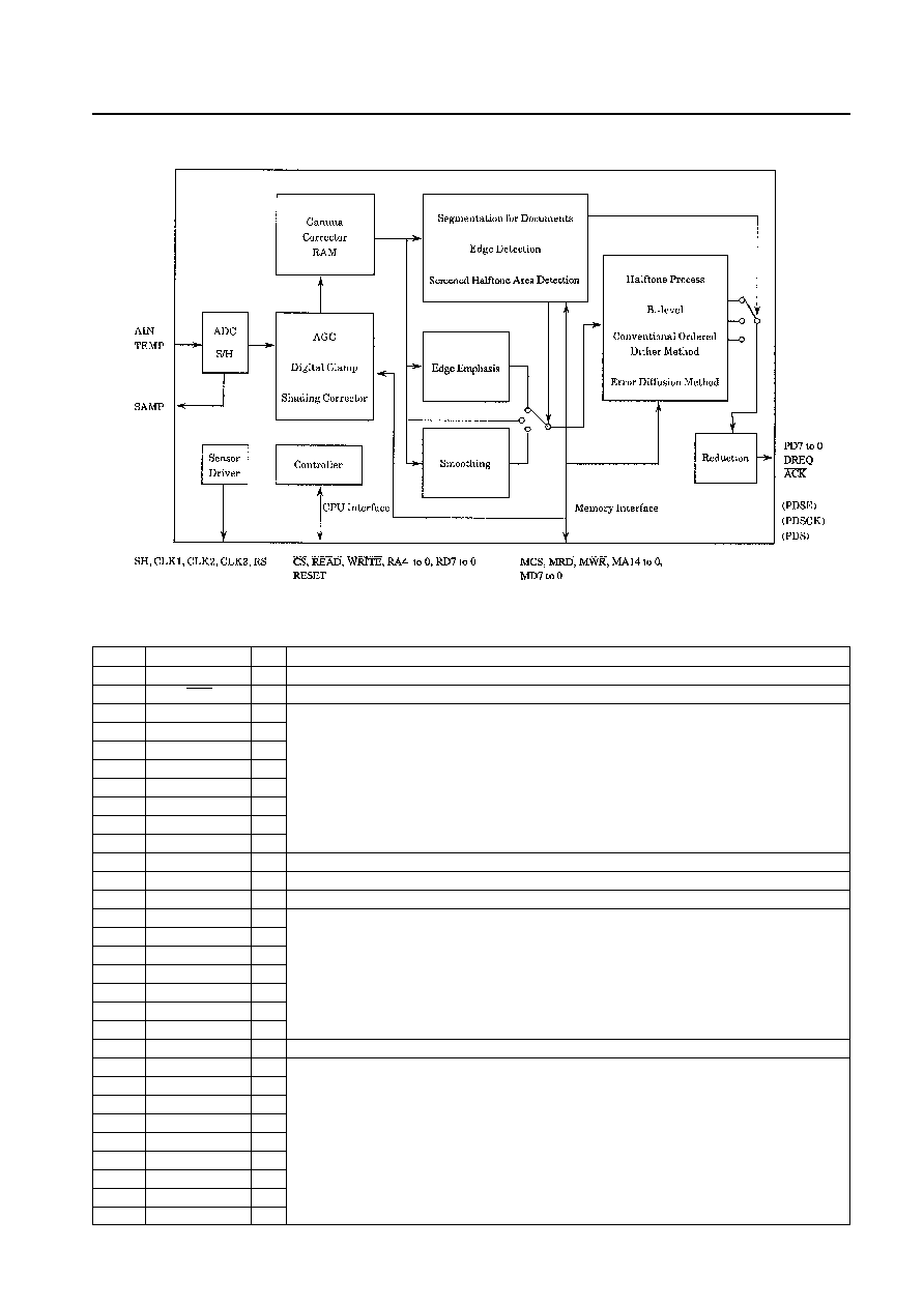
Block Diagram
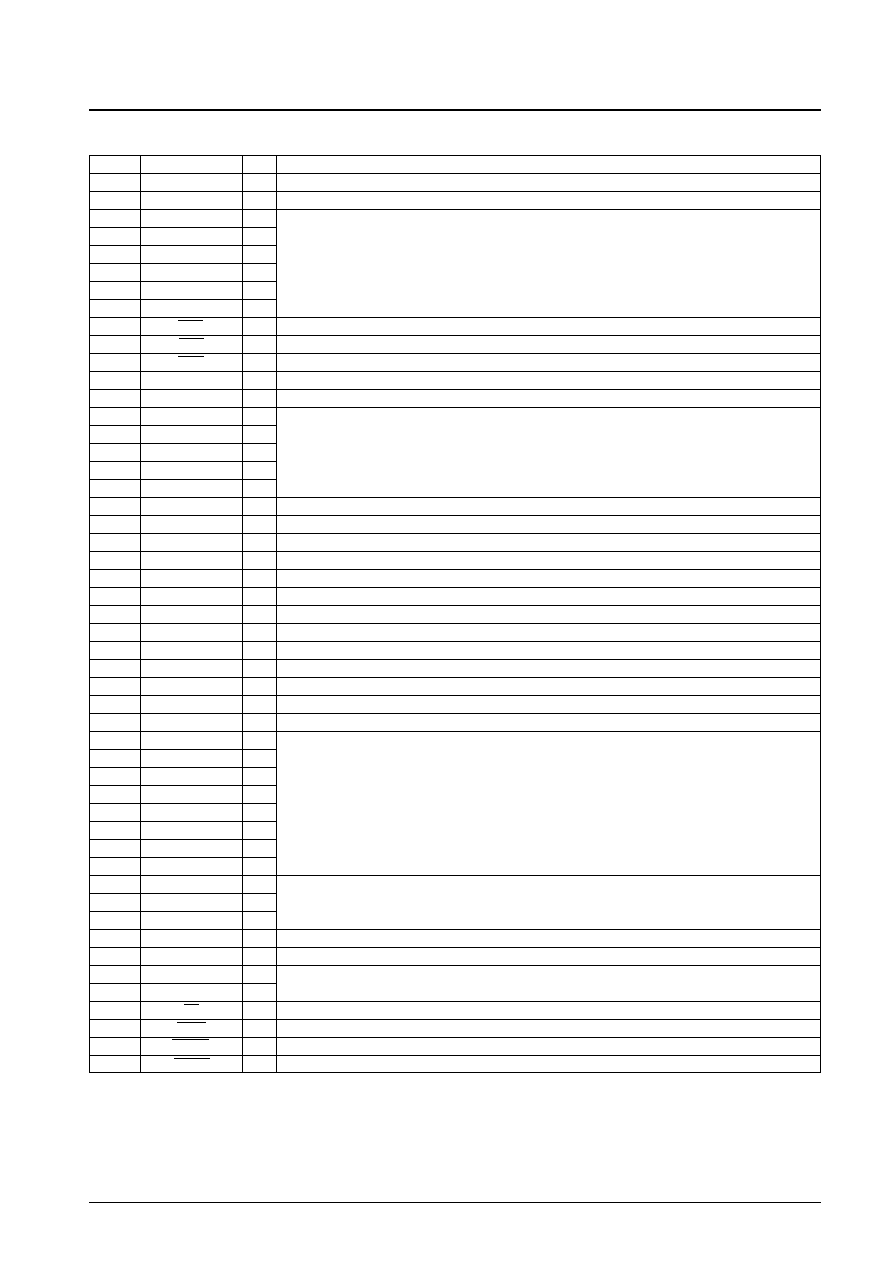
Pin Functions
Type: I: Input pin, O: Output pin, B: Bidirectional pin, P: Power supply pin, NC: No connection
No. 4982-2/5
LC82101
Pin No.
Symbol
I/O
Function
1
DREQ
O
DMA data request signal output
2
ACK
I
DMA acknowledge signal input
3
PD0
O
4
PD1
O
Binary image data parallel data bus
5
PD2
O
The data order is set by the MSBF register.
6
PD3
O
7
PD4
O
8
PD5/SDE
O
Pin 8 can be switched to function as the serial data output valid period signal.
9
PD6/SDCK
O
Pin 9 can be switched to function as the serial data transfer clock.
10
PD7/SD
O
Pin 10 can be switched to function as the serial data output.
11
MD0
B
External memory data bus
12
DV
DD
P
Digital system power supply
13
DGND
P
Digital system ground
14
MD1
B
15
MD2
B
16
MD3
B
External memory data bus
17
MD4
B
MD7 is the MSB and MD0 is the LSB.
18
MD5
B
19
MD6
B
20
MD7
B
21
DGND
P
Digital system ground
22
MA0
O
23
MA1
O
24
MA2
O
25
MA3
O
External memory address
26
MA4
O
MA14 is the MSB and MA0 is the LSB.
27
MA5
O
28
MA6
O
29
MA7
O
30
MA8
O
Continued on next page.
Continued from preceding page.
Type: I: Input pin, O: Output pin, B: Bidirectional pin, P: Power supply pin, NC: No connection
No. 4982-3/5
LC82101
Pin No.
Symbol
I/O
Function
31
DV
DD
P
Digital system power supply
32
DGND
P
Digital system ground
33
MA9
O
34
MA10
O
35
MA11
O
External memory address bus
36
MA12
O
MA14 is the MSB and MA0 is the LSB.
37
MA13
O
38
MA14
O
39
MCS
O
External memory CS signal
40
MRD
O
External memory READ signal
41
MWR
O
External memory WRITE signal
42
DGND
P
Digital system ground
43
MTP
O
Motor drive timing signal output
44
SH
O
45
RS
O
46
CLK1
O
Sensor drive signal outputs
47
CLK2
O
48
CLK3
O
49
SAMP
O
Sampling clock monitor
50
CLKIN
I
System clock input
51
DV
DD
P
Digital system power supply
52
DGND
P
Digital system ground
53
NC
NC
54
NC
NC
55
NC
NC
56
TEST
I
Test input (Connect to ground in normal use.)
57
AGND
P
Analog system ground
58
ATAP
O
Analog mid-level connection
59
AIN
I
Sensor signal input
60
TEMP
I
Temperature signal input
61
AV
DD
P
Analog system power supply
62
RD0
B
63
RD1
B
64
RD2
B
65
RD3
B
CPU interface data bus
66
RD4
B
RD7 is the MSB and RD0 is the LSB.
67
RD5
B
68
RD6
B
69
RD7
B
70
RA0
I
CPU interface address bus
71
RA1
I
RA4 is the MSB and RA0 is the LSB.
72
RA2
I
73
DV
DD
P
Digital system power supply
74
DGND
P
Digital system ground
75
RA3
I
CPU interface address bus
76
RA4
I
77
CS
I
CPU interface CS signal
78
READ
I
CPU interface READ signal
79
WRITE
I
CPU interface WRITE signal
80
RESET
I
System reset
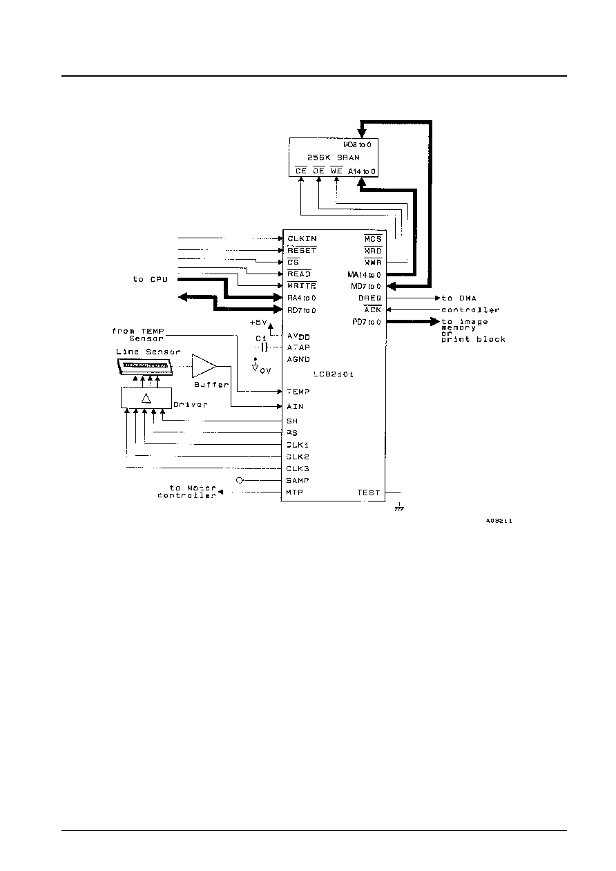
Sample Application Circuit
1. C1: Use a 0.01 µF laminated ceramic capacitor.
2. Set up the polarity of the image signal from the sensor so that white data is represented by the highest potential and
black data by the lowest potential. A level conversion circuit can allow the whole dynamic range of the built-in A/D
converter to be used effectively if the maximum output level of the peaks in the image signal from the sensor does
not reach 4.2 V.
3. When a 64 K SRAM is used as the distortion correction memory, leave MA11 and MA12 unused and connect MA13
and MA14 to the memory A11 and A12 lines.
4. Although AGND and DGND are completely isolated internally in this LSI, AV
DD
and DV
DD
are connected through
the substrate. Therefore, the power supply system must be designed so that no potential difference between AV
DD
and DV
DD
can occur. Also, when power is applied or removed, the time lag between the power supplies must be
under 3 ms.
No. 4982-4/5
LC82101
PS No. 4982-5/5
LC82101
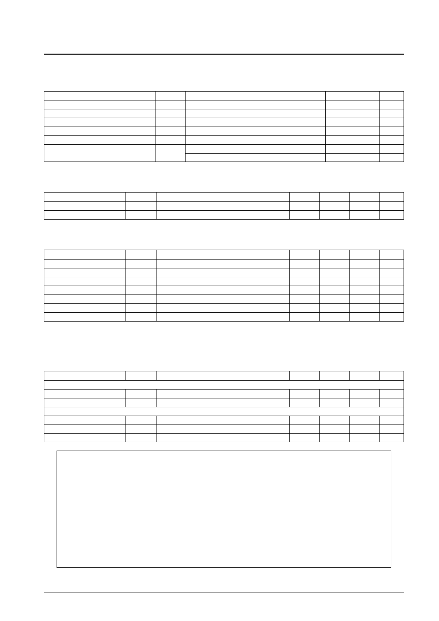
Specifications
Absolute Maximum Ratings
at Ta = 25∞C, GND = 0 V
Allowable Operating Conditions
at Ta = ≠30 to +70∞C, GND = 0 V
DC Characteristics
at Ta = ≠30 to +70∞C, GND = 0 V, V
DD
= 4.5 to 5.5 V
Analog Characteristics
The minimum signal level in analog input signals must be matched to AGND, and the maximum signal level must
not exceed the maximum AGC potential.
This catalog provides information as of June, 1995. Specifications and information herein are subject to change
without notice.
s
No products described or contained herein are intended for use in surgical implants, life-support systems, aerospace
equipment, nuclear power control systems, vehicles, disaster/crime-prevention equipment and the like, the failure of
which may directly or indirectly cause injury, death or property loss.
s
Anyone purchasing any products described or contained herein for an above-mentioned use shall:
Accept full responsibility and indemnify and defend SANYO ELECTRIC CO., LTD., its affiliates, subsidiaries and
distributors and all their officers and employees, jointly and severally, against any and all claims and litigation and all
damages, cost and expenses associated with such use:
Not impose any responsibility for any fault or negligence which may be cited in any such claim or litigation on
SANYO ELECTRIC CO., LTD., its affiliates, subsidiaries and distributors or any of their officers and employees
jointly or severally.
s
Information (including circuit diagrams and circuit parameters) herein is for example only; it is not guaranteed for
volume production. SANYO believes information herein is accurate and reliable, but no guarantees are made or implied
regarding its use or any infringements of intellectual property rights or other rights of third parties.
Parameter
Symbol
Conditions
Ratings
Unit
Maximum supply voltage
V
DD
max
≠0.3 to +7.0
V
I/O voltages
V
I
, V
O
≠0.3 to V
DD
+ 0.3
V
Allowable power dissipation
Pd max
Ta
70∞C
450
mW
Operating temperature
Topr
≠30 to +70
∞C
Storage temperature
Tstg
≠55 to +125
∞C
Soldering conditions
Hand soldering: 3 seconds
350
∞C
Reflow soldering: 10 seconds
235
∞C
Parameter
Symbol
Conditions
min
typ
max
Unit
Supply voltage
V
DD
4.5
5.5
V
Input voltage
V
IN
0
V
DD
V
Parameter
Symbol
Conditions
min
typ
max
Unit
Input high-level voltage
V
IH
2.2
V
Input low-level voltage
V
IL
0.8
V
Input leakage current
I
L
V
IN
= V
DD
, V
SS
≠25
+25
µA
Output high-level voltage
V
OH
I
OH
= 3 mA
2.4
V
Output low-level voltage
V
OL
I
OL
= 3 mA
0.4
V
Output leakage current
I
L
When in the high-impedance state
≠100
+100
µA
Current drain
I
DD
V
DD
= 5.0 V, SYSCLK = 32 MHz
40
60
mA
Parameter
Symbol
Conditions
min
typ
max
Unit
[When AGND = 0 V]
Maximum potential
0.82
0.84
0.86
AV
DD
V
Minimum potential
0.22
0.24
0.26
AV
DD
V
[When AV
DD
= 5.0 V, AGND = 0 V, and the AGC is at the maximum potential]
Resolution
8
bit
Linearity error
±1
LSB
Differential linearity error
±1
LSB