 | –≠–ª–µ–∫—Ç—Ä–æ–Ω–Ω—ã–π –∫–æ–º–ø–æ–Ω–µ–Ω—Ç: LC82102W | –°–∫–∞—á–∞—Ç—å:  PDF PDF  ZIP ZIP |
CMOS LSI
Ordering number : EN
*
5155
91195HA (OT) No. 5155-1/5
Preliminary
SANYO Electric Co.,Ltd. Semiconductor Bussiness Headquarters
TOKYO OFFICE Tokyo Bldg., 1-10, 1 Chome, Ueno, Taito-ku, TOKYO, 110-8534 JAPAN
Image-Processing LSI
for Fax, Copier and OCR Products
LC82102, LC82102W
Overview
The LC82102 and LC82102W convert analog video
signals from CCD or contact image sensors to high-
quality binary video data. The LC82102/W converts the
input analog data to multi-valued data and uses two-
dimensional filtering and an error diffusion technique that
produces high-quality images to produce a two-valued
image. Finally, the LC82102 reduces the image in the
main and subsidiary scan directions. The LC82102
requires absolutely no external memory since it limits the
number of pixels processed to 2040 per line. This LSI can
implement the image processing used by FAX, copier and
OCR products.
Features
∑ Number of pixels processed: 2040 pixels/line
∑ Processing speed: 500 ns/pixel maximum (when the
CLKIN input frequency is 32 MHz)
∑ Built-in 8-bit A/D converter (includes a sensor signal
delay adjustment function)
∑ Built-in 6-bit D/A converter for setting the A/D
converter high reference potential
∑ Sensor drive circuit (supports CCD and all CIS types)
∑ Digital clamp (single-point clamp, even/odd clamp)
∑ Distortion correction (white correction: 8-pixel
averaging correction, black correction: black correction
subtraction data setting)
∑ Gamma correction (supports user-defined curves)
∑ Simple binary-conversion processing (fixed threshold
level, density-adaptive threshold level)
∑ Intermediate processing error diffusion (64 levels)
∑ Image reduction (thinning, fine black line retaining, fine
white line retaining)
∑ Single-voltage 5 V supply and low power due to CMOS
process fabrication
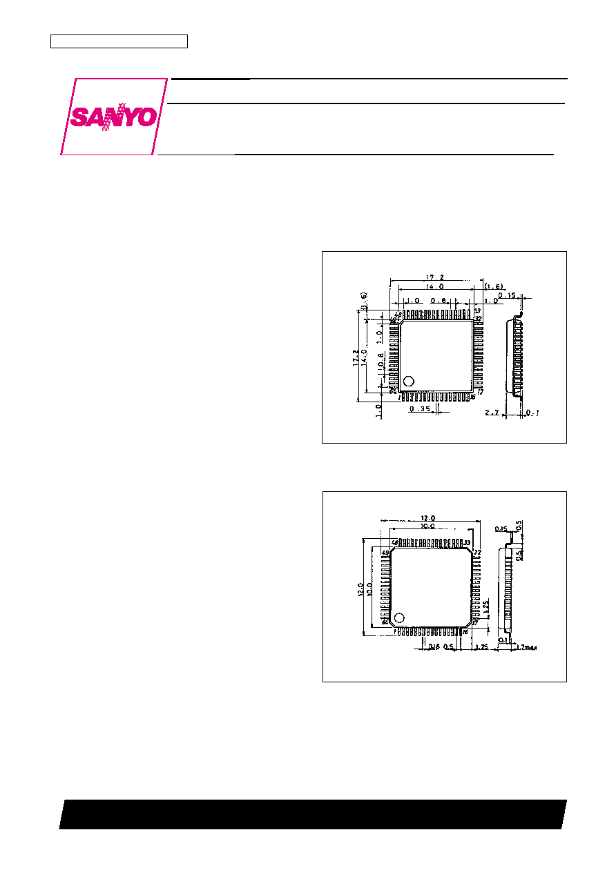
Package Dimensions
unit: mm
3159-QFP64E
unit: mm
3190-SQFP64
SANYO: SQFP64
[LC82102W]
[LC82102]
SANYO: QIP64E

Specifications
Absolute Maximum Ratings
at Ta = 25∞C, GND = 0 V
Allowable Operating Ranges
at Ta = ≠30 to +70∞C, GND = 0 V
DC Characteristics
at Ta = ≠30 to +70∞C, GND = 0 V, V
DD
= 4.5 to 5.5 V
Analog Characteristics
No. 5155-2/5
LC82102, LC82102W
Parameter
Symbol
Conditions
Ratings
Unit
Maximum supply voltage
V
DD
max
≠0.3 to +7.0
V
Maximum I/O voltages
V
I
, V
O
max
≠0.3 to V
DD
+ 0.3
V
Allowable power dissipation
Pd max
Ta
70∞C
350
mW
Operating temperature
Topr
≠30 to +70
∞C
Storage temperature
Tstg
≠55 to +125
∞C
Soldering conditions
Hand soldering: 3 seconds
350
∞C
Reflow soldering: 10 seconds
235
∞C
Parameter
Symbol
Conditions
min
typ
max
Unit
Supply voltage
V
DD
4.5
5.5
V
Input voltage
V
IN
0
V
DD
V
Parameter
Symbol
Conditions
min
typ
max
Unit
Input high level voltage
V
IH
2.2
V
Input low level voltage
V
IL
0.8
V
Input leakage current
I
L
V
IN
= V
DD
, V
SS
≠25
+25
µA
Output high level voltage
V
OH
I
OH
= ≠3 mA
2.4
V
Output low level voltage
V
OL
I
OL
= 3 mA
0.4
V
Output leakage current
I
L
For high-impedance output
≠100
+100
µA
Current drain
I
DD
CLKIN = 32 MHz
40
70
mA
Parameter
Symbol
Conditions
min
typ
max
Unit
[D/A Converter]
Resolution
6
bit
Internal resistance
5.0
k
[A/D Converter] when ADREFL = 0 V, and the ATAP potential is 4.2 V
Resolution
8
bit
Linearity error
±1
LSB
Differential linearity error
±1
LSB
Internal resistance
300
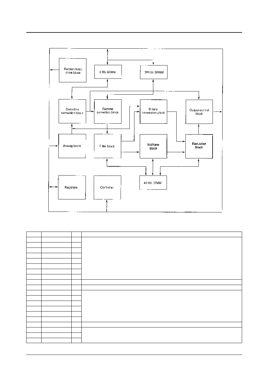
Block Diagram
Pin Functions
Type: I: Input pin, O: Output pin, B: Bidirectional pin, P: Power supply pin, NC: No connection
No. 5155-3/5
LC82102, LC82102W
Pin No.
Symbol
I/O
Function
1
D7
B
2
D6
B
3
D5
B
4
D4
B
CPU interface data bus
5
D3
B
D7 is the MSB and D0 is the LSB.
6
D2
B
7
D1
B
8
D0
B
9
DGND
P
Digital system ground
10
DV
DD
P
Digital system power supply
11
A8
I
12
A7
I
13
A6
I
CPU interface address bus
14
A5
I
A8 is the MSB and A0 is the LSB.
15
A4
I
16
A3
I
17
DGND
P
Digital system ground
18
A2
I
19
A1
I
CPU interface address bus
20
A0
I
Continued on next page.
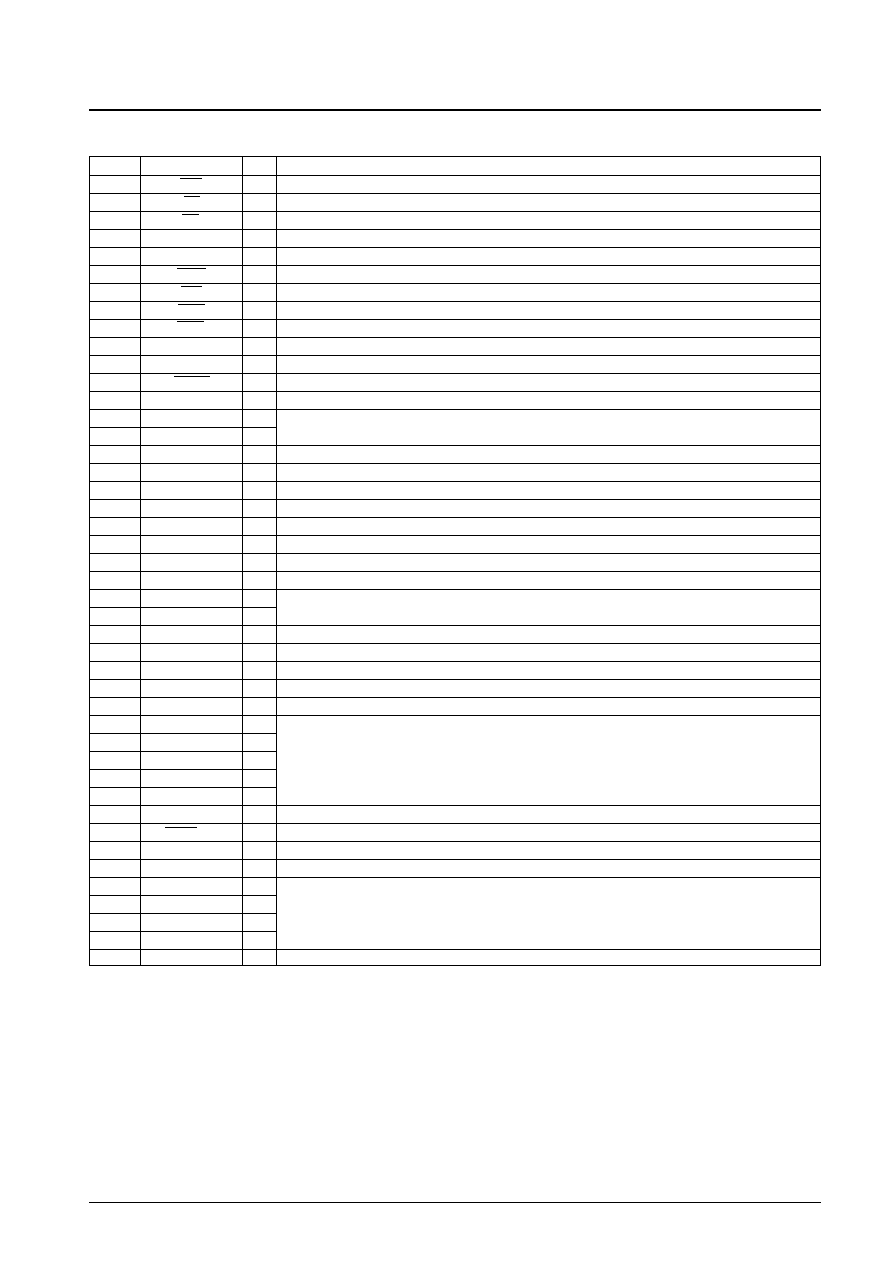
Continued from preceding page.
Type: I: Input pin, O: Output pin, B: Bidirectional pin, P: Power supply pin, NC: No connection
No. 5155-4/5
LC82102, LC82102W
Pin No.
Symbol
I/O
Function
21
WR
I
CPU interface write signal
22
RD
I
CPU interface read signal
23
ME
I
CPU interface memory enable signal
24
DV
DD
P
Digital system power supply
25
CLKIN
I
System clock input
26
TEST
I
Test pin (Connect to ground in normal use.)
27
IOE
I
CPU interface I/O enable signal
28
MCS
I
CPU interface memory chip select signal
29
IOCS
I
CPU interface I/O chip select signal
30
ICLK
I
External sampling point signal input
31
TRIG
I
External trigger signal input
32
RESET
I
System reset
33
SAMP/LININT
O
A/D converter sampling point monitor signal output/LINE signal output
34
AP3
O
General-purpose analog ports
35
AP2
O
36
AGND
P
Digital system ground
37
ADREFL
I
A/D converter low reference voltage
38
DAREFL
I
D/A converter low reference voltage
39
AIN
I
Sensor signal input
40
TEMP
I
Temperature signal input
41
ATAP
O
Intermediate analog connection
42
DAREFH
I
D/A converter high reference voltage
43
AV
DD
P
Analog system power supply
44
AP1
O
General-purpose analog ports
45
AP0
O
46
AGND
P
Analog system ground
47
PD7/SD
B
DMA output/serial data output
48
PD6/SDCK
B
DMA output/serial data transfer clock
49
DGND
P
Digital system ground
50
PD5/SDE
B
DMA output/serial data output valid signal
51
PD4/PP4
B
52
PD3/PP3
B
53
PD2/PP2
B
DMA output/general-purpose I/O ports
54
PD1/PP1
B
55
PD0/PP0
B
56
DV
DD
P
Digital system power supply
57
DACK/PP5
B
DMA data acknowledge signal input/general-purpose I/O port
58
DREQ/PP5
B
DMA data request signal output/general-purpose I/O port
59
MTP/PP7
B
Motor drive timing signal output/general-purpose I/O port
60
CLK2
O
61
CLK1
O
Sensor drive signal output
62
RS
O
63
SH
O
64
DGND
P
Digital system ground

PS No. 5155-5/5
LC82102, LC82102W
This catalog provides information as of September, 1995. Specifications and information herein are subject to
change without notice.
s
No products described or contained herein are intended for use in surgical implants, life-support systems, aerospace
equipment, nuclear power control systems, vehicles, disaster/crime-prevention equipment and the like, the failure of
which may directly or indirectly cause injury, death or property loss.
s
Anyone purchasing any products described or contained herein for an above-mentioned use shall:
Accept full responsibility and indemnify and defend SANYO ELECTRIC CO., LTD., its affiliates, subsidiaries and
distributors and all their officers and employees, jointly and severally, against any and all claims and litigation and all
damages, cost and expenses associated with such use:
Not impose any responsibility for any fault or negligence which may be cited in any such claim or litigation on
SANYO ELECTRIC CO., LTD., its affiliates, subsidiaries and distributors or any of their officers and employees
jointly or severally.
s
Information (including circuit diagrams and circuit parameters) herein is for example only; it is not guaranteed for
volume production. SANYO believes information herein is accurate and reliable, but no guarantees are made or implied
regarding its use or any infringements of intellectual property rights or other rights of third parties.
Sample Application
1. C1: Use a 0.01 µF laminated ceramic capacitor.
2. Set up the polarity of the image signal from the sensor so that white data is represented by the highest potential and
black data by the lowest potential. A level conversion circuit can allow the whole dynamic range of the built-in A/D
converter to be used effectively if the maximum output level of the peaks in the image signal from the sensor does
not reach 4.2 V.
3. Although AGND and DGND are completely isolated internally in this LSI, AV
DD
and DV
DD
are connected through
the substrate. Therefore, the power supply system must be designed so that no potential difference between AV
DD
and DV
DD
can occur. Also, when power is applied or removed, the time lag between the power supplies must be
under 3 ms.