 | –≠–ª–µ–∫—Ç—Ä–æ–Ω–Ω—ã–π –∫–æ–º–ø–æ–Ω–µ–Ω—Ç: LC82211T | –°–∫–∞—á–∞—Ç—å:  PDF PDF  ZIP ZIP |
Ordering number : ENN
*
6349
51200RM (OT)/30899TH (OT) No. 6349-1/5
Overview
The LC82211T is a high-speed JPEG codec that support
motion JPEG. The encode function compresses digital
video (YUV422) in real time and the decode function
expands compressed code data and outputs a digital video
signal. The LC82211T can support a wide range of digital
video applications including cameras and video capture
systems. Since the LC82211T includes 4 megabits of
image memory (DRAM) on chip, it can significantly
reduce the mounting area required for this functionality.
Features
∑ Implements encoding and decoding based on the JPEG
standard.
∑ Processes 640
◊
480 pixel images at 30 frames per
second.
∑ On-chip image memory (4M DRAM)
∑ Image memory compression function that reduce image
memory requirements by one half.
∑ The capture and display image size, and the compression /
expansion image size can be set to arbitrary values
independently.
∑ Image memory can be accessed from the CPU bus.
∑ YUV422 to YUV420 subsampling function
∑ DMA transfer support. Single mode, demand mode, and
Hitachi SH mode are supported.
∑ Maximum operating clock frequency: 18 MHz
∑ Supply voltage: 3.3 V
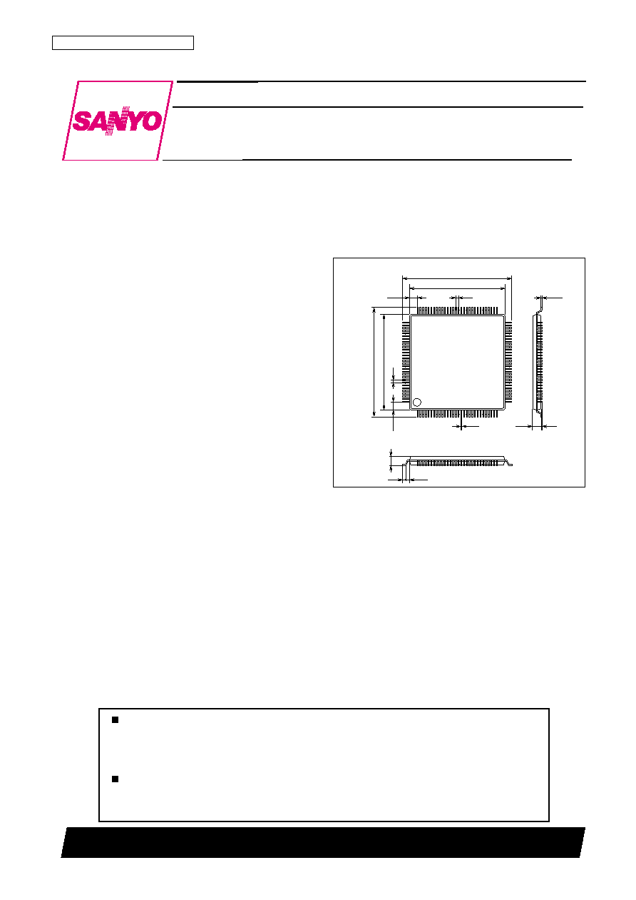
∑ Package: TQFP-120
Package Dimensions
unit: mm
3257-TQFP120
Preliminary
LC82211T
SANYO Electric Co.,Ltd. Semiconductor Company
TOKYO OFFICE Tokyo Bldg., 1-10, 1 Chome, Ueno, Taito-ku, TOKYO, 110-8534 JAPAN
Motion JPEG Codec
CMOS IC
120
1
30
31
60
61
90
91
0.4
14.0
(1.2)
(0.5)
0.125
16.0
0.5
0.15
1.2max
0.1
0.4
14.0
(1.2)
(1.0)
16.0
SANYO: TQFP120
[LC82211T]
Any and all SANYO products described or contained herein do not have specifications that can handle
applications that require extremely high levels of reliability, such as life-support systems, aircraft's
control systems, or other applications whose failure can be reasonably expected to result in serious
physical and/or material damage. Consult with your SANYO representative nearest you before using
any SANYO products described or contained herein in such applications.
SANYO assumes no responsibility for equipment failures that result from using products at values that
exceed, even momentarily, rated values (such as maximum ratings, operating condition ranges, or other
parameters) listed in products specifications of any and all SANYO products described or contained
herein.

No. 6349-2/5
LC82211T
CPU
I/F
L1
FIFO
L2 FIFO
32 words
◊
2
Video
FIFO
Sub
Sampler
Video
I/F
DRAM I/F
4 Mbit-DRAM
JPEG CORE
=Working with PIXCLK
D[15 : 0]
A[1 : 0]
CPUTYPE
ZCS
ZRD
ZWR
RDY
ZDRQ
ZDACK
DRAK
ZIRQ
ZRESET
TEST
ZPDN
CLK
CLKSEL
DIR
HACTIVE
VSYNC
HSYNC
PIXCLK
FIELD
PXEN
C[7 : 0]
Y[7 : 0]
ZWE
MA
MD
ZCAS
ZRAS
A12867
Block Diagram
No. 6349-3/5
LC82211T
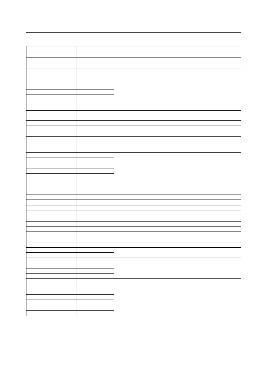
Pin Functions
Pin No.
Pin
I/O
Attribute
Function
1
V
DD
P
--
2
CLK
I
--
Clock input
3
ZRESET
I
S
Reset
4
ZWE
O
--
DRAM Write Enable (Connected internally)
5
ZRAS0
O
--
DRAM RAS0 (Connected internally)
6
ZRAS1
O
--
DRAM RAS1 (Unused)
7
MA0
O
--
8
MA1
O
--
DRAM Address (Connected internally)
9
MA2
O
--
10
MA3
O
--
11
V
DD
P
--
12
CPUTYPE
I
--
0: Intel Mode, 1: Motorola Mode
13
DRAK
I
S
Hitachi SH series DRAK
14
V
SS
P
--
15
V
DD
P
--
16
V
SS
P
--
17
V
DD
P
--
18
V
SS
P
--
19
V
DD
P
--
20
MA4
O
--
21
MA5
O
--
22
MA6
O
--
DRAM address (Connected internally)
23
MA7
O
--
24
MA8
O
--
25
MA9
O
--
26
ZOE
O
--
DRAM Output Enable (Connected internally)
27
ZCASH
O
--
DRAM CASH (Connected internally)
28
ZCASL
O
--
DRAM CASL (Connected internally)
29
ZIRQ
O
--
Interrupt request
30
V
SS
P
--
31
V
DD
P
--
32
ZCS
I
S
Chip select
33
ZWR/ZDS
I
S
Intel: WR, Motolora: DS
34
ZRD/RW
I
S
Intel: RD, Motolora: RW
35
ZDRQ
O
--
DMA Request
36
ZDACK
I
S
DMA Acknowledge
37
RDY
O
--
Intel: Ready, Motolora: DTACK
38
A1
I
--
CPU Address
39
A0
I
--
40
D0
I/O
--
41
D1
I/O
--
CPU Data
42
D2
I/O
--
43
D3
I/O
--
44
V
SS
P
--
45
V
DD
P
--
46
D4
I/O
--
47
D5
I/O
--
48
D6
I/O
--
CPU Data
49
D7
I/O
--
50
D8
I/O
--
Continued on next page.

No. 6349-4/5
LC82211T
Continued from preceding page.
Pin No.
Pin
I/O
Attribute
Function
51
D9
I/O
--
CPU Data
52
V
SS
P
--
53
V
DD
P
--
54
D10
I/O
--
55
D11
I/O
--
56
D12
I/O
--
CPU Data
57
D13
I/O
--
58
D14
I/O
--
59
D15
I/O
--
60
V
SS
P
--
GND
61
V
DD
P
--
V
DD
62
ZPDN
I
--
Power down
63
MD8
I/O
R
64
MD9
I/O
R
DRAM data (Connected internally)
65
MD10
I/O
R
66
MD11
I/O
R
67
V
DD
P
--
68
V
SS
P
--
69
MD12
I/O
R
70
MD13
I/O
R
DRAM data (Connected internally)
71
MD14
I/O
R
72
CLKSEL
I
--
Clock selection 0: No divider circuit, 1: Divider circuit used
73
MD15
I/O
R
DRAM data (Connected internally)
74
V
SS
P
--
75
TEST
I
--
Test or clock selection (see note)
76
V
SS
P
--
77
V
DD
P
--
78
MD0
I/O
R
DRAM data (Connected internally)
79
V
DD
P
--
80
MD1
I/O
R
81
MD2
I/O
R
DRAM data (Connected internally)
82
MD3
I/O
R
83
V
DD
P
--
84
V
SS
P
--
85
MD4
I/O
R
86
MD5
I/O
R
DRAM data (Connected internally)
87
MD6
I/O
R
88
MD7
I/O
R
89
DIR
O
--
Video bus I/O direction
90
V
SS
P
--
91
V
DD
P
--
92
C0/R0
I/O
R
93
C1/R1
I/O
R
Video data
94
C2/R2
I/O
R
95
C3/R3
I/O
R
96
C4/R4
I/O
R
Video data
97
C5/B0
I/O
R
98
V
SS
P
--
99
V
DD
P
--
100
C6/B1
I/O
R
Video data
Continued on next page.

PS No. 6349-5/5
LC82211T
This catalog provides information as of May, 2000. Specifications and information herein are subject to
change without notice.
Specifications of any and all SANYO products described or contained herein stipulate the performance,
characteristics, and functions of the described products in the independent state, and are not guarantees
of the performance, characteristics, and functions of the described products as mounted in the customer's
products or equipment. To verify symptoms and states that cannot be evaluated in an independent device,
the customer should always evaluate and test devices mounted in the customer's products or equipment.
SANYO Electric Co., Ltd. strives to supply high-quality high-reliability products. However, any and all
semiconductor products fail with some probability. It is possible that these probabilistic failures could
give rise to accidents or events that could endanger human lives, that could give rise to smoke or fire,
or that could cause damage to other property. When designing equipment, adopt safety measures so
that these kinds of accidents or events cannot occur. Such measures include but are not limited to protective
circuits and error prevention circuits for safe design, redundant design, and structural design.
In the event that any or all SANYO products (including technical data, services) described or contained
herein are controlled under any of applicable local export control laws and regulations, such products must
not be exported without obtaining the export license from the authorities concerned in accordance with the
above law.
No part of this publication may be reproduced or transmitted in any form or by any means, electronic or
mechanical, including photocopying and recording, or any information storage or retrieval system,
or otherwise, without the prior written permission of SANYO Electric Co., Ltd.
Any and all information described or contained herein are subject to change without notice due to
product/technology improvement, etc. When designing equipment, refer to the "Delivery Specification"
for the SANYO product that you intend to use.
Information (including circuit diagrams and circuit parameters) herein is for example only; it is not
guaranteed for volume production. SANYO believes information herein is accurate and reliable, but
no guarantees are made or implied regarding its use or any infringements of intellectual property rights
or other rights of third parties.
Continued from preceding page.
Pin No.
Pin
I/O
Attribute
Function
101
C7/B2
I/O
R
Video data
102
Y0/B3
I/O
R
Video data
103
Y1/B4
I/O
R
104
V
SS
P
--
105
V
DD
P
--
106
Y2/G0
I/O
R
107
Y3/G1
I/O
R
108
Y4/G2
I/O
R
Video data
109
Y5/G3
I/O
R
110
Y6/G4
I/O
R
111
Y7/G5
I/O
R
112
V
SS
P
--
113
V
DD
P
--
114
VSYNC
I
--
Vertical sync signal
115
HSYNC
I
--
Horizontal sync signal
116
PIXCLK
I
--
Pixel clock
117
FIELD
I
--
Field signal
118
PXEN
I
--
Pixel enable (1: Enable, 0: Disable)
119
HACTIVE
O
--
Horizontal active period output
*
1
120
V
SS
P
--
Notes:
∑ Signal names starting with Z are active-low signals. Signal names starting with S are Schmitt inputs, and those starting with R have a built-in pull-up resistor.
∑ Clock internal divider mode
TEST/CLKSEL3
CLKSEL
MODE
0
0
No internal divider
0
1
Internally divided by 2
1
1
Internally divided by 3
1
0
Test mode
Note:
*
1. This signal goes low during the vertical blanking period.