Overview
The LC82220 is a single-chip JPEG decoder designed for
wide range of digital video playback applications
including amusement systems, video games and PC JPEG
playback cards. The LC82220 is capable of decoding
JPEG bitstreams of SIF resolution with a picture rate of 30
frames/sec. The digital video output can be formatted for
NTSC, PAL, SECAM, or any other optional video
standard. The complete decoding function is realised with
the LC82220, a standard 8-bit or 16-bit microcontroller
and a bank of DRAM. A typical memory configuration is
a single 128 k
◊
16 or 256 k
◊
16 DRAM. The LC82220
also supports efficient video display functions such as
scroll and overlay.
Functions
∑
Support for JPEG format
∑
Real-time decoding of motion-JPEG with rate of 30
frames/sec
∑
Lowest solution cost for amusement, game, PC
systems
∑
Support for YUV 4:1:1 color format
∑
YUV or RGB digital video outputs compatible with
optional video format
∑
Programmable picture and display window format
∑
Support for trick display: scrolling, overlaying
∑
Standard 8/16-bit microcontroller interface with DMA
support for compressed data input
∑
Support SOI and EOI markers
∑
Direct connect to video DAC
∑
Direct connect to 2 M or 4 M DRAM as bit and frame
buffers
∑
Two Q-tables included
∑
High-speed processing by fixed Huffman tables
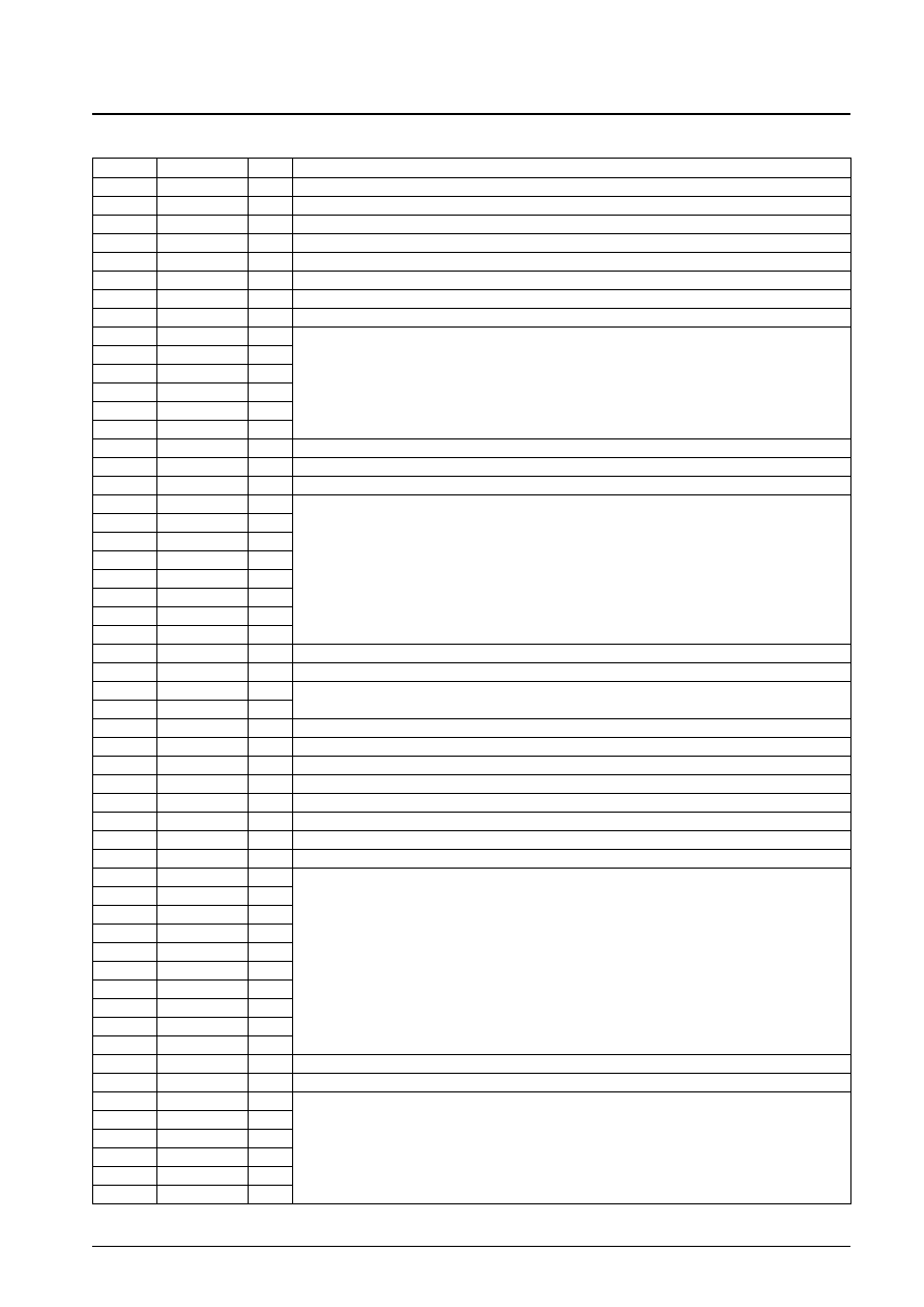
Package Dimensions
unit: mm
3182-QFP128E
CMOS LSI
62096HA (OT) No. 5422-1/6
Preliminaly
SANYO: QIP128E
[LC82220]
SANYO Electric Co.,Ltd. Semiconductor Bussiness Headquarters
TOKYO OFFICE Tokyo Bldg., 1-10, 1 Chome, Ueno, Taito-ku, TOKYO, 110 JAPAN
Motion JPEG Decoder LSI
LC82220
Ordering number : EN
*
5422
No. 5422-3/6
LC82220
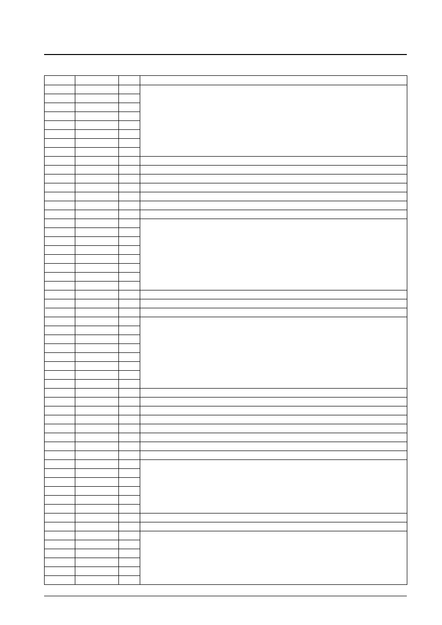
Pin Functions
Pin No.
Symbol
I/O
Function
1
V
DD
+5 V power supply
2
ZCTLINT
O
Control bus interrupt request (open drain output)
3
ZCTLCS
I
Control bus select
4
ZCTLRD
I
Control bus read or R/W select
5
ZCTLWR
I
Control bus write or Data strobe
6
ZCTLRDY
O
Control bus ready (tristate output)
7
TEST3
I
Test pin
8
TEST4
I
Test pin
9
CTLA5
I
10
CTLA4
I
11
CTLA3
I
Control bus address
12
CTLA2
I
13
CTLA1
I
14
CTLA0
I
15
CTLCPU
I
Control bus CPU type selection
16
V
DD
+5 V power supply
17
V
SS
Ground
18
CTLD7
I/O
19
CTLD6
I/O
20
CTLD5
I/O
21
CTLD4
I/O
Control bus data
22
CTLD3
I/O
23
CTLD2
I/O
24
CTLD1
I/O
25
CTLD0
I/O
26
TEST0
I
Test pin
27
ZRESET
I
Hardware reset
28
CLKSEL0
I
Clock divisor setting
29
CLKSEL1
I
CLKSEL1:0 = 00: no divisor, 01: clock divided by 2, 10: clock divided by 3
30
CLK
I
System (decode) clock input (CMOS level input)
31
TEST1
I
Test pin
32
V
DD
+5 V power supply
33
V
SS
Ground
34
ZCDCS/ZCDACK
I
Code bus select or Code bus DMA acknowledge
35
ZCDINT/ZCDREQ
O
Code bus interrupt or Code bus DMA request
36
ZCDWR
I
Code bus data write signal
37
ZCDRDY
O
Code bus ready (tristate output)
38
CCD15
I
39
CCD14
I
40
CCD13
I
41
CCD12
I
42
CCD11
I
Code bus data
43
CCD10
I
44
CCD9
I
45
CCD8
I
46
CCD7
I
47
CCD6
I
48
V
SS
Ground
49
V
DD
+5 V power supply
50
CCD5
I
51
CCD4
I
52
CCD3
I
Code bus data
53
CCD2
I
54
CCD1
I
55
CCD0
I
Continued on next page.
No. 5422-4/6
LC82220
Continued from preceding page.
Pin No.
Symbol
I/O
Function
56
DB7
O
57
DB6
O
58
DB5
O
59
DB4
O
Pixel data bus B (V)
60
DB3
O
61
DB2
O
62
DB1
O
63
DB0
O
64
V
SS
Ground
65
V
DD
+5V power supply
66
ZBLANK
O
Blanking signal
67
ZPXEN
I
Pixel data enable signal
68
PXCLK
I
Pixel clock
69
ZVSYNC
I
Vertical synchronizing signal
70
ZHSYNC
I
Horizontal synchronizing signal
71
DG7
O
72
DG6
O
73
DG5
O
74
DG4
O
Pixel data bus G (U)
75
DG3
O
76
DG2
O
77
DG1
O
78
DG0
O
79
TEST2
I
Test pin
80
V
DD
+5 V power supply
81
V
SS
Ground
82
DR7
O
83
DR6
O
84
DR5
O
85
DR4
O
Pixel data bus R (Y)
86
DR3
O
87
DR2
O
88
DR1
O
89
DR0
O
90
V
SS
Ground
91
ZOE
O
Memory output enable
92
ZWEL
O
Memory write enable (L)
93
ZRAS
O
Row address strobe
94
ZCASL
O
Column address strobe (L)
95
ZWEH/ZCASH
O
Memory write enable (H)/column address strobe (H)
96
V
DD
+5 V power supply
*
1
97
V
SS
Ground
98
MD15
I/O
99
MD14
I/O
100
MD13
I/O
Frame memory interface data bus
101
MD12
I/O
102
MD11
I/O
103
MD10
I/O
104
V
DD
+5 V power supply
105
V
SS
Ground
106
MD9
I/O
107
MD8
I/O
108
MD7
I/O
Frame memory interface data bus
109
MD6
I/O
110
MD5
I/O
111
MD4
I/O
Continued on next page.
No. 5422-5/6
LC82220
Continued from preceding page.
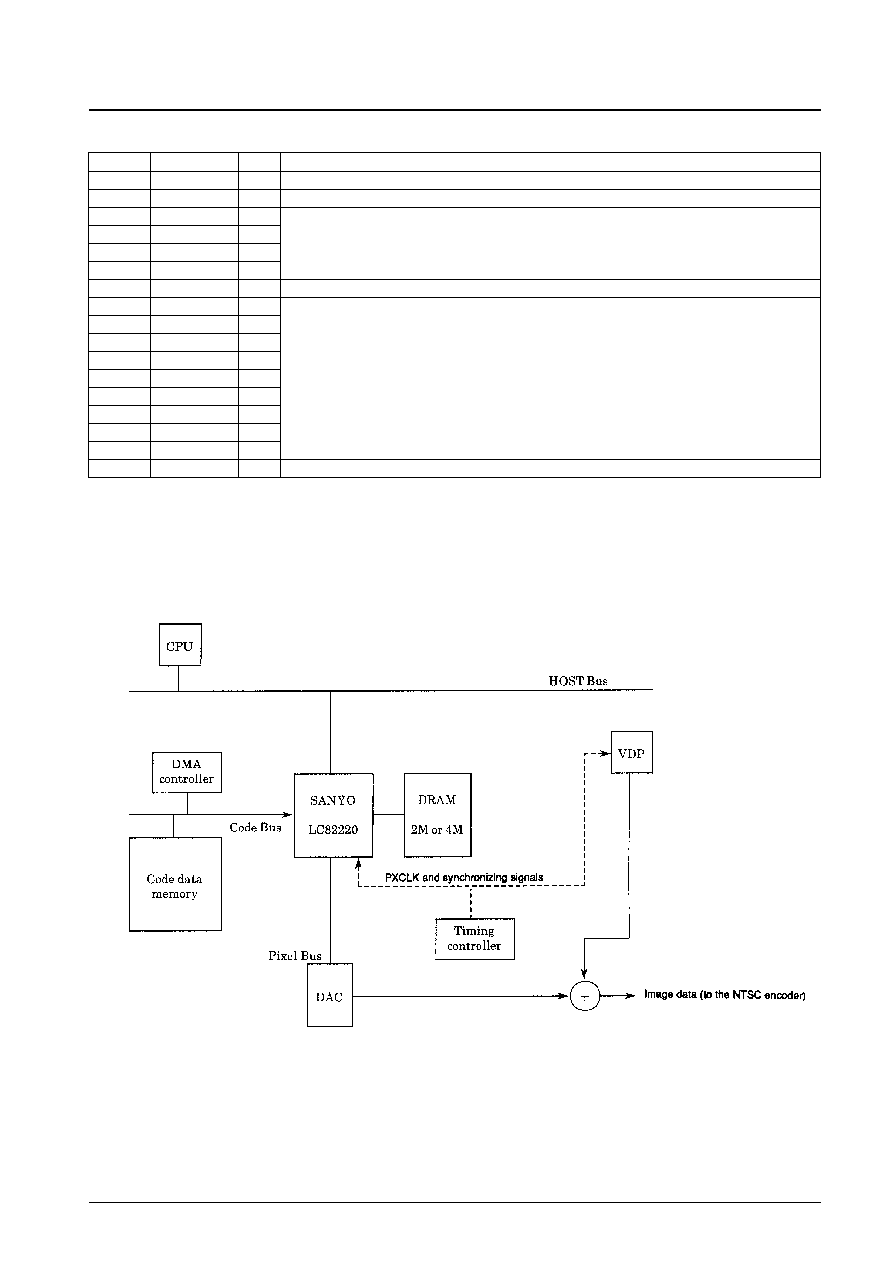
System Configuration Example
1. Separate code bus type
This is a system in which the code and system busses are separated. The coded data input does not load down the
system bus.
Pin No.
Symbol
I/O
Function
112
V
SS
Ground
113
V
DD
+5 V power supply
114
MD3
I/O
115
MD2
I/O
Frame memory interface data bus
116
MD1
I/O
117
MD0
I/O
118
V
SS
Ground
119
MA8
O
120
MA7
O
121
MA6
O
122
MA5
O
123
MA4
O
Frame memory address signals
124
MA3
O
125
MA2
O
126
MA1
O
127
MA0
O
128
V
SS
Ground